CXSD62130 CXSD62130A is a 1.5MHz high efficiency monolithic synchronous buck regulator. Design with current mode scheme,the CXSD62130 CXSD62130A is stable
with ceramic output capacitor. Input voltage from 2.7V to 6.0V makes the
CXSD62130 CXSD62130A ideally suited for single Li-Ion battery powered
applications. 100%duty cycle provides low dropout operation, extending
battery life in portable electrical devices. Theinternally fixed 1.5MHz
operating frequency allows the using of small surface mount inductors and capacitors. The synchronous switches included inside increase the efficiency
and eliminate the need of an external Schottky diode.
-
"
目录
1.产品概述 2.产品特点
3.应用范围 4.下载产品资料PDF文档
5.产品封装图 6.电路原理图
7.功能概述 8.相关产品
一,产品概述(General Description)
CXSD62130 CXSD62130A is a 1.5MHz high efficiency monolithic synchronous buck regulator. Design with current mode scheme,the CXSD62130 CXSD62130A is stable
with ceramic output capacitor. Input voltage from 2.7V to 6.0V makes the
CXSD62130 CXSD62130A ideally suited for single Li-Ion battery powered
applications. 100%duty cycle provides low dropout operation, extending
battery life in portable electrical devices. Theinternally fixed 1.5MHz
operating frequency allows the using of small surface mount inductors and capacitors. The synchronous switches included inside increase the efficiency
and eliminate the need of an external Schottky diode.
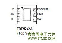
The CXSD62130 CXSD62130A is available in TDFN2x2-6 packages.
二.产品特点(Features)
1A Output Current
Wide 2.7V~6.0V Input Voltage
Fixed 1.5MHz Switching Frequency
Low Dropout Operating at 100% Duty Cycle
25μA Quiescent Current
Synchronous Rectifier
0.6V Reference Voltage
<0.5μA Input Current During Shutdown
Short-Circuit Protection
Over-Temperature Protection
Available in TDFN2x2-6 Packages
Lead Free and Green Devices Available
(RoHS Compliant)
三,应用范围 (Applications)
HD STB
BT Mouse
PND Instrument
Portable Instrument
四.下载产品资料PDF文档
需要详细的PDF规格书请扫一扫微信联系我们,还可以获得免费样品以及技术支持!

五,产品封装图 (Package)
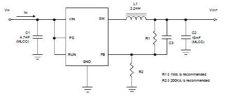
六.电路原理图
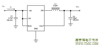
七,功能概述
Main Control Loop
The CXSD62130 CXSD62130A is a constant frequency, synchronous rectifier and current-mode
switching regulato r. In normal operation, the internal P-channel power MOSFET is turned on each
cycle. The peak inductor current at which ICMP turn off the P-FET is controlled by the voltage on
the COMP node, which is the output of the error amplifier (EAMP). An external resistive divider
connected between VOUT and ground allows the EAMP to receive an output feedback voltage
VFB at FB pin. When the load current increases, it causes a slightly decrease in VFB relative to
the 0.6V reference, which in turn causes the COMP voltage to increase until the average
inductor current matches the new load current.
Enable/Shutdown
Driving RUN to the ground places the CXSD62130 CXSD62130A in shutdown mode. When
in shutdown, the internal power MOSFETs turn off, all internal circuitry shuts down and the
quiescent supply current reduces to 0.5μA maximum.
Pulse Frequency Modulation Mode (PFM)
The CXSD62130 CXSD62130A is a fixed frequency, peak current mode PWM step-down
converter. At light loads, the CXSD62130 CXSD62130A will automatically enter in pulse
frequency mode operation to reduce the dominant switching losses. In PFM operation,
the inductor current may reach zero or reverse on each pulse. A zero current comparator
turn off the N-FET, forcing DCM operation at light load. These controls get very low
quiescent current, help to maintain high effi-ciency over the complete load range.
Slope Compensation and Inductor Peak Current
The CXSD62130 CXSD62130A is a peak current mode PWM step downconverter. To
prevent sub-harmonic oscillations, theCXSD62130 CXSD62130A sense the peak current and
add slope compensation to stable the converter. It is accomplished in-ternally by adding
a compensating ramp to the inductor current signal at duty cycles in excess of 40%.
Normally,this results in a reduction of maximum inductor peak current for duty cycles >
40%. However, the CXSD62130 CXSD62130A uses a special scheme that counteracts this
compensating ramp, which allows the maximum inductor peak current to remain unaffected
throughout all duty cycles.
Dropout Operation
As the input supply voltage decreases to a value ap-proaching the output voltage, the duty
cycle increases toward the maximum on time. Further, reduction of thesupply voltage forces
the main switch to remain on for more than one cycle until it reaches 100% duty cycle. The
input voltage minus the voltage drop will determine the output voltage across the P-FET
and the inductor.An important detail to remember is that on resistance of P-FET switch
will increase at low input supply voltageTherefore, the user should calculate the power dissipa-
tion when the CXSD62130 CXSD62130A is used at 100% duty cycle with low input voltage.
Over-Temperature Protection (OTP)
The over-temperature circuit limits the junction tempera-ture of the CXSD62130 CXSD62130A.
When the junction temperature ex-ceeds 150oC, a thermal sensor turns off the both power
MOSFETs, allowing the devices to cool. The thermal sen-sor allows the converters to start a
soft-start process and regulate the output voltage again after the junction tem-perature cools
by 30oC. The OTP is designed with a 30oC hysteresis to lower the average Junction
Temperature (TJ) during continuous thermal overload conditions, in-creasing the lifetime
of the device.
八,相关产品 更多同类产品.......
|
Switching Regulator > Buck Converter |
|||||||||||
|
Part_No |
Package |
Architectu |
No.of PWM Outpu |
Drive Lout (A) |
Vin(V) |
Fmax Khz |
Vref (V) |
R-Top (milohm) |
R-Sync (milohm) |
Iq (No load) (uA) |
|
|
min |
max |
||||||||||
|
TQFN5x6-28 |
CM |
1 |
5 |
4.5 |
26 |
380 |
0.8 |
50 |
20 |
1000 |
|
|
SOP-8 |
CM |
1 |
2 |
4.5 |
26 |
380 |
0.8 |
100 |
1000 |
||
|
SOP-8P |
CM |
1 |
4 |
4.5 |
26 |
380 |
0.8 |
80 |
1000 |
||
|
SOT23-5|TSOT23-5 |
CM |
1 |
1 |
2.7 |
6 |
1500 |
0.6 |
280 |
250 |
25 |
|
|
SOT23-5 |
CM |
1 |
1 |
2.7 |
6 |
1500 |
0.6 |
280 |
250 |
||
|
SOP-8 |
CM |
1 |
3 |
4.3 |
14 |
500 |
0.8 |
70 |
70 |
500 |
|
|
SOP-8P |
CM |
1 |
3 |
4.3 |
14 |
500 |
0.8 |
55 |
45 |
500 |
|
|
TDFN3x3-10 |
3 |
2.6 |
5.5 |
2000 |
0.8 |
110 |
110 |
460 |
|||
|
TDFN3x3-10 |
CM |
2 |
1 |
2.7 |
6 |
1500 |
0.6 |
280 |
250 |
500 |
|
|
TDFN3x3-10 |
CM |
2 |
1 |
2.7 |
6 |
1500 |
0.6 |
280 |
250 |
||
|
TDFN2x2-6 |
CM |
1 |
1 |
2.7 |
6 |
1500 |
0.6 |
280 |
250 |
25 |
|
|
TDFN2x2-6 |
CM |
1 |
1 |
2.7 |
6 |
1500 |
0.6 |
280 |
250 |
||
|
TDFN3x3-12 |
CM |
2 |
1 |
2.7 |
6 |
1500 |
0.6 |
280 |
250 |
25 |
|
|
TDFN3x3-12 |
CM |
2 |
1 |
2.7 |
6 |
1500 |
0.6 |
280 |
250 |
||
|
TDFN 3x3 12 |
CM |
2 |
1 |
3 |
5.5 |
1500 |
0.6 |
280 |
250 |
30 |
|
|
TQFN3x3-20 |
CM |
3 |
2 |
2.9 |
5.5 |
1500 |
0.6 |
- |
- |
300 |
|
|
TDFN2x2-8 |
CM |
1 |
1 |
3.3 |
8 |
1500 |
0.6 |
280 |
250 |
25 |
|
|
SOP-8 |
CM |
1 |
2 |
4.5 |
24 |
340 |
0.925 |
110 |
110 |
1900 |
|
|
SOP-8P |
CM |
1 |
3 |
4.5 |
24 |
340 |
0.925 |
||||