燙XLC8981 CXLC8982 includes one time programmable (OTP) memory to store the DAC code on the chip, eliminating the need for external EEPROM. The chip supports up to 100 write operations to OTP memory. CXLC8981 CXLC8982 has an I 2 C interface to set the VCOM reference voltage and write into OTP memory.The CXLC8981 CXLC8982 provides a programmable reference voltage for TFT-LCD panel VCOM adjustment

-
[ CXLC8981 ]"
目录
7.相关产品
产品概述 返回TOP
CXLC8981 CXLC8982 includes one time programmable (OTP) memory to store the DAC code on the chip, eliminating the need for external EEPROM. The chip supports up to 100 write operations to OTP memory. CXLC8981 CXLC8982 has an I 2 C interface to set the VCOM reference voltage and write into OTP memory.The CXLC8981 CXLC8982 provides a programmable reference voltage for TFT-LCD panel VCOM adjustment. A 7-bit digital-to-analog converter (DAC) detects current from an external resistor-divider to create the VCOM reference voltage. This voltage is used as the input to a high current drive voltage buffer.
产品特点 返回TOP
„ Integrated Nonvolatile Memory to Store VCOM Setting
„ 100 Programming Times
„ I 2 C Interface
„ 7-Bit, Adjustable Sink-Current Device
„ Resistor-Adjustable, Full-Scale Range
„ 2.5V to 3.6V Logic Supply Range
„ 7V to 18V Analog Supply Range
„ Protections:
Š Over Current Protection (OCP)
Š Over Temperature Protection (OTP)
„ TDFN3X3-8 Package
„ RoHS Compliant
应用范围 返回TOP
„ TFT-LCD Panels
技术规格书(产品PDF) 返回TOP
需要详细的PDF规格书请扫一扫微信联系我们,还可以获得免费样品以及技术支持!

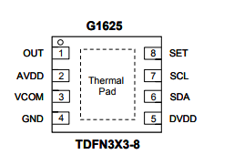
产品封装图 返回TOP

电路原理图 返回TOP
a
相关芯片选择指南 返回TOP 更多同类产品......
|
ntegrated Buffer |
|||||||||
|
Part NO. |
VDD (V) min |
VDD (V) max |
CH Vr+ Vcom |
IOUT (mA) Vr,Vcom |
S/R (V/μs) Vr,Vcom |
BW (MHz) Vr,Vcom |
ISC (mA) Vr,Vcom |
Note |
Package |
|
6.5 |
18 |
1 |
100 |
20 |
19 |
260 |
SMBus, Rail-to-Rail Output |
TDFN3X3-10 |
|
|
9 |
20 |
14+1 |
25, 100 |
16, 70 |
10, 19 |
100, 260 |
Rail-to-Rail Output, SMBus,2 Banks MTP |
QFN5X5-32 |
|
|
6.5 |
19.5 |
18+1 |
30, 100 |
16, 80 |
9, 15 |
120, 300 |
Rail-to-Rail Output |
TQFP7X7-48/(FD) |
|
|
6.5 |
19.5 |
14+1 |
30, 100 |
16, 80 |
9, 15 |
120, 300 |
Rail-to-Rail Output |
TQFP7X7-48/(FD) |
|
|
7 |
20 |
12+1 |
25, 100 |
16, 50 |
30 |
100, 300 |
Rail-to-Rail Output, SMBus,2 Banks REG |
QFN4X4-24 |
|
|
7 |
20 |
16+2 |
25, 100 |
16, 50 |
30 |
100, 300 |
Rail-to-Rail Output, SMBus,2 Banks MTP |
QFN5X5-28 |
|
|
7 |
20 |
12+1+1 |
25, 100 |
16, 50 |
30 |
100, 300 |
Rail-to-Rail Output, SMBus,Banks MTP, CRC |
QFN4X4-24 |
|
|
6.5 |
18 |
14+1 |
25, 100 |
20, 20 |
10, 20 |
75, 140 |
Rail-to-Rail Output,SMBus ,2 Banks MTP, Checksum |
TQFN5X5-32 |
|
|
7 |
18 |
1 |
100 |
23 |
20 |
270 |
SMBus,Rail-to-Rail Output |
TDFN3X3-8 |
|
|
7 |
18 |
1 |
100 |
-- |
-- |
-- |
SMBus, VCOM REF |
TDFN3X3-8 |
|
|
7 |
20 |
8+1 |
25, 100 |
16, 50 |
30 |
100, 300 |
SMBus, Rail-to-Rail Output,2 Bank MTP |
QFN4X4-24 |
|


