The CXCO4331 integrated one VGON boost converter with a high voltage level shifter. This device is suitable for GOA TFT-LCD panel applications. The VGON boost converter is a current mode regulator with a temperature compensation feature. The output voltage is adjusted according to the voltage on the VT pin (temperature reading) and the voltage level is set by voltage reference on the END pin
-
[ CXCO4331 ]"
目录
7.相关产品
产品概述 返回TOP
The CXCO4331 integrated one VGON boost converter with a high voltage level shifter. This device is suitable for GOA TFT-LCD panel applications. The VGON boost converter is a current mode regulator with a temperature compensation feature. The output voltage is adjusted according to the voltage on the VT pin (temperature reading) and the voltage level is set by voltage reference on the END pin. This boost converter has an integrated 45V/1.3Ω NMOS switch and a fixed 600kHz switching frequency. It provides fast transient response to pulsed loading while achieving efficiency over 85%. The level shifters transform the logic-level controlled signals, which are generated by the display timing controller (TCON), into the high-level signals needed by LCD panel. Different CKH1~6 output patterns will be generated by different external settings. Each channel of level shifter output uses low impedance transistors to achieve fast rising and falling time, even when driving the capacitive loads present in LCD applications. CXCO4331 can also be used as a stand-alone level shifter. Connecting SHD to GND can disable whole boost function, shut down function, temperature compensation function, UVP, OCP except for XON function. CXCO4331eatures extensive protection functions that include UVLO, OVP, UVP, OCP and OTP. The device operates over the temperature range of -40°C to +85°C. CXCO4331s available in a 5mmx5mm 40-lead TQFN Package.
产品特点 返回TOP
„ Input Supply Range: 2.6V~5.5V
„ Current Mode Boost Controller for VGON
Š Fixed 600kHz Switching Frequency
Š Integrated 45V/1.5A,1.3Ω Switching NMOS
Š Input voltage, VINP=4.5V to 15V
Š Output Voltage, VGON = 17V to 39V
Š Up 80% Efficiency (5mA < Load Current)
Š Up 75% Efficiency (100mA < Load Current)
Š 2% Output Regulation
„ Built-In Power on Sequence and Soft Start Function
„ Protection Function
Š Input Under Voltage Lockout (UVLO)
Š Thermal Overload Protection (TOP)(150°C)
Š Output Over Voltage Protection for VGON (OVP) (39V)
Š Over Current Protection for VGON (OCP) (1.5A typ.)
Š Output Under Voltage Protection (UVP) (FBG≦0.8V)
„ Thermal Compensation Function
Š VGON temperature compensation
Š Vcom temperature compensation
„ 10-Channel Level Shifter
Š +45V Highest Voltage Level
Š -30V Lowest Voltage Level
Š Maximum 700ns Rising/Falling Time
Š 500mA Peak Current
Š 20mA Continuous Current
„ 40-pin, TQFN(5mmx5mm) Package
„ RoHS Compliant
应用范围 返回TOP
„ GOA TFT-LCD Panel
技术规格书(产品PDF) 返回TOP
需要详细的PDF规格书请扫一扫微信联系我们,还可以获得免费样品以及技术支持!

产品封装图 返回TOP

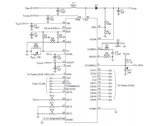
电路原理图 返回TOP
相关芯片选择指南 返回TOP 更多同类产品。。。。。。
|
Level Shifter |
|||||||||
|
Part NO. |
VDD(V min. |
VDD(V max. |
CH |
IOUT (mA) |
VLOW (V) |
VHIGH (V) |
S/R (ns) |
Note |
Package |
|
6 |
16 |
5 |
50 |
0 |
18 |
25 |
2 Vcom buffers |
TQFN5X5-32 |
|
|
-- |
-- |
8 |
500 |
-35 |
35 |
12 |
VGH1-VGL 6-CH,VGH2-VGL 2-CH |
TSSOP20/TQFN4X4-20 |
|
|
2.6 |
5.5 |
10 |
500 |
-30 |
40 |
700 |
Gate Power |
TQFN5X5-40 |
|
|
1.2 |
5.5 |
2001-2-4 |
-- |
1.2 |
5 |
17 |
1-2-4-Bit Bidirectional Level Shift, Push-Pull Input/Ouput |
SC70-6/SOT23-6/ AQFN1.7X2.0-12 |
|
|
2.6 |
5.5 |
9 |
-- |
-30 |
40 |
-- |
N/A |
TQFN5X5-40 |
|
|
1.2 |
5 |
2 |
-- |
1.2 |
5 |
-- |
1-Bit, 2-Bit Bidirectional I2C Bus&Voltage-Level Shift, Open drain Input/Ouput |
SC70-6/TDFN3X2-8/ADF N3X2-8/AQFN1.5X1.5-8 |
|
|
1.65 |
5 |
4 |
-- |
1.8 |
5 |
240 |
4-Bit Bidirectional Level-Shift,Open Drain Input/Ouput |
WLCSP3X4-12 |
|
|
1.2 |
5 |
1 |
-- |
1.2 |
5 |
-- |
1-Bit,2-Bit Bidirectional I2C Bus &Voltage-Level Shift,Open drain Input/Ouput |
SC70-6/TDFN3X2-8/ADF N3X2-8/AQFN1.5X1.5-8 |
|


