CXAC85191 is a highly integrated current mode PWM control IC optimized for high performance, low standby power and cost effective offline flyback converter applications. PWM switching frequency at normal operation is externally programmable and trimmed to tight range. At no load or light load condition, the IC operates in extended ‘burst mode’ to minimize switching loss. Lower standby power and higher conversion efficiency is thus achieved. VDD low startup current and low operating current contribute to a reliable power on startup design with CXAC85191. A large value resistor could thus be used in the startup circuit to minimize the standby power. The internal slope compensation improves system large signal stability and reduces the possible sub-harmonic oscillation at high PWM duty cycle output. Leading-edge blanking on current sense input removes the signal glitch due to snubber circuit diode reverse recovery. This greatly helps to reduce the external component count and system cost in application. CXAC85191 offers complete protection coverage with automatic self-recovery feature including Cycle-by-Cycle current limiting (OCP), over load protection (OLP), over temperature protection (OTP), VDD over voltage protection (OVP) and under voltage lockout (UVLO). The Gate-drive output is clamped at 18V to protect the power MOSFET
-
[ CXAC85191 ]"
目录
7.相关产品
产品概述 返回TOP
CXAC85191是一种高度集成的电流型PWM控制芯片,对高性能、低待机功率和低成本的离线反激转换器应用程序进行了优化。正常操作的PWM开关频率在外部可编程,并被调整到窄幅。在无负载或轻载状态下,芯片以扩展的“间歇振荡模式”运行,以减少开关损耗。从而实现了较低的待机功率和更高的转换效率。VDD低启动电流和低工作电流在启动设计上CXAC85191提供了可靠的电源。因此,可以在启动电路中使用一个比较大电阻来减小待机功率。内部的斜波补偿提高了系统的大信号稳定性,降低了高PWM工作周期输出可能的二次谐波振荡。在电流检测输入端的前沿消隐消除了由于阻尼电路二极管反向恢复而产生的信号故障。这极大地减少了应用程序中的外部器件数量和系统成本。
CXAC85191提供了完善的保护功能模块,自动恢复功能包括周期循环的过流保护(OCP)、过载保护(OLP)、超温保护(OTP)、VDD过电压保护(OVP)和低电压锁定(UVLO)。为了保护功率MOSFET,Gate驱动输出箝位在18V。
在CXAC85191中,OCP阈值斜率在内部优化,达到了通用交流输入范围的恒定输出功率极限。
优良的EMI特性是在图腾柱门驱动输出中实现抖频技术和软开关控制。
在工作中20KHZ以下的音频能量最小化,因此音频噪声的性能得到了很大的提高。
CXAC85191提供了SOP8和DIP8封装。
CXAC85191 is a highly integrated current mode PWM control IC optimized for high performance, low standby power and cost effective offline flyback converter applications. PWM switching frequency at normal operation is externally programmable and trimmed to tight range. At no load or light load condition, the IC operates in extended ‘burst mode’ to minimize switching loss. Lower standby power and higher conversion efficiency is thus achieved. VDD low startup current and low operating current contribute to a reliable power on startup design with CXAC85191. A large value resistor could thus be used in the startup circuit to minimize the standby power. The internal slope compensation improves system large signal stability and reduces the possible sub-harmonic oscillation at high PWM duty cycle output. Leading-edge blanking on current sense input removes the signal glitch due to snubber circuit diode reverse recovery. This greatly helps to reduce the external component count and system cost in application. CXAC85191 offers complete protection coverage with automatic self-recovery feature including Cycle-by-Cycle current limiting (OCP), over load protection (OLP), over temperature protection (OTP), VDD over voltage protection (OVP) and under voltage lockout (UVLO). The Gate-drive output is clamped at 18V to protect the power MOSFET. In CXAC85191, OCP threshold slope is internally optimized to reach constant output power limit over universal AC input range. Excellent EMI performance is achieved frequency shuffling technique together with soft switching control at the totem pole gate drive output. The tone energy at below 20KHZ is minimized in operation. Consequently, audio noise erformance is greatly improved. CXAC85191 is offered in both SOP-8 and DIP-8 packages
产品特点 返回TOP
增强式突发模式控制为提高效率和最小待机功率设计;
无噪声操作;
外置可调整的PWM开关频率;
内置同步斜率补偿;
低VIN / VDD启动电流(6.5 ua)和低工作电流(2.3mA);
在电流检测输入上内置前沿消隐;
完善的保护和自动恢复功能;
外置可调整的过温保护(OTP);
内置OVP和UVLO保护;
Gate输出最大电压箝位(18V);
内置周期循环的过流保护(OCP);
内置过载保护(OLP);
采用SOP8和DIP8封装。
◆ Extended Burst Mode Control For Improved Efficiency and Minimum Standby Power Design.
◆ Audio Noise Free Operation
◆ External Programmable PWM Switching Frequency
◆ Internal Synchronized Slope Compensation
◆ Low VIN/VDD Startup Current(6.5uA) and Low Operating Current (2.3mA)
◆ Leading Edge Blanking on Current Sense Input
◆ Complete Protection Coverage With Auto Self-Recovery
◆ External Programmable Over Temperature Protection (OTP)
◆ On-chip VDD OVP for System OVP Under Voltage Lockout with Hysteresis (UVLO)
◆ Gate Output Maximum Voltage Clamp (18V)
◆ Line Compensated Cycle-by-Cycle Over-current Threshold Setting For Constant Output Current Limiting Over Universal Input Voltage Range (OCP)
◆ Over Load Protection. (OLP)
应用范围 返回TOP
◆ Laptop Power Adaptor
◆ PC/TV/Set-Top Box Power
◆ Supplies Open-frame SMPS
◆ Battery Charge
技术规格书(产品PDF) 返回TOP
需要详细的PDF规格书请扫一扫微信联系我们,还可以获得免费样品以及技术支持!

产品封装图 返回TOP

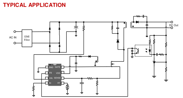
电路原理图 返回TOP
相关芯片选择指南 返回TOP 更多同类产品.....
|
AC-DC |
||||||||
|
型号 |
封装 |
开关管 |
最大功率 |
待机功率 |
工作模式 |
最大Vcc电压 |
最大工作频率 |
拓扑 |
|
SOP7 |
700V BJT |
2.5W |
<100mW |
PFM |
8.5V |
100KHZ |
PSR |
|
|
SOP7 |
800V BJT |
5W |
<100mW |
PFM |
8.5V |
100KHZ |
PSR |
|
|
SOP7 |
800V BJT |
10W |
<100mW |
PFM |
8.5V |
100KHZ |
PSR |
|
|
DIP7 |
800V BJT |
10W |
<100mW |
PFM |
8.5V |
100KHZ |
PSR |
|
|
SOP5 |
800V BJT |
5W |
<100mW |
PFM |
8.5V |
100KHZ |
PSR |
|
|
TO126 |
650V BJT |
4W |
<300mW |
PFM |
7V |
60KHZ |
PSR |
|
|
TO126 |
700V BJT |
5W |
<300mW |
PFM |
7V |
60KHZ |
PSR |
|
|
TO126 |
700V BJT |
5W |
<300mW |
PFM |
7V |
60KHZ |
PSR |
|
|
SOP8 |
600V MOS |
5W |
<200mW |
PWM |
26V |
70KHz |
PSR |
|
|
DIP8 |
600V MOS |
10W |
<200mW |
PWM |
30V |
60KHZ |
PSR |
|
|
SOP8 |
外置 |
100W |
<300mW |
PWM |
30V |
65KHZ |
SSR |
|
|
SOT23-6 |
外置 |
30W |
<200mW |
PWM |
30V |
65kHz |
SSR |
|
|
DIP8 |
外置 |
200W |
<300mW |
PWM |
16V |
52kHz |
SSR |
|
|
DIP8 |
外置 |
200W |
<300mW |
PWM |
16V |
52kHz |
SSR |
|
|
SOP8 |
外置 |
200W |
<300mW |
PWM |
16V |
52kHz |
SSR |
|
|
SOP8 |
外置 |
200W |
<300mW |
PWM |
16V |
52kHz |
SSR |
|


