The cxld6410 uses charge transfer technology to realize the step-down operation, and the efficiency is twice as high as the normal linear voltage regulator. Different from the common DCDC, the external inductance of the switch is required, which brings about the RF interference problem. The cxld6410 uses the capacitor to carry out charge transfer to improve the efficiency, avoid the interference problem, and at the same time, when the load is lower than 50mA, the efficiency is generally higher than that of the DCDC. The cxld6410 maintains a very small output ripple and a static power consumption of 150ua. Integrated over-voltage protection, over temperature protection, over-current protection and other functions. It is the best choice of 12V input to low-voltage output in the system, considering both efficiency and switching RF interference
-
"
目录
1.产品概述 2.产品特点 3.应用范围 4.技术规格书下载(PDF文档)
一.产品概述
CXLD6410是利用电荷转移技术,实现降压工作时,效率比通常的线性稳压器提升一倍。不同于普通的DCDC,需要开关外围电感,从而带来的射频干扰问题,CXLD6410利用电容进行电荷转移来提升效率,避免了干扰问题的同时,在带载低于50mA时,效率还普遍高于DCDC。CXLD6410同时维持了很小的输出纹波,150uA的静态功耗。集成了过压保护,过热保护,过流保护等功能。是系统中12V输入转低压输出,要兼顾效率和开关射频干扰的最佳选择。
二.产品特点
◆宽输入范围4.4-16V
◆最高输出电压5V
◆最大输出电流400mA
◆最高耐压20V
◆反馈电压1.1V
◆效率比传统线性稳压器高一倍
◆无需电感
◆SOP8封装
三.应用范围
◆无线射频传输模块
◆电力线载波模块
◆智能家居
四.技术规格书(产品PDF)
需要详细的PDF规格书请扫一扫微信联系我们,还可以获得免费样品以及技术支持!

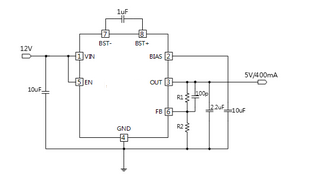
五.产品封装图


六.电路原理图
七.相关芯片选择指南
| LDO | ||||||||
| Device | Device | Architecture | VIN | VOUT | IOUT | Vfb | ||
| Description | (min) | (max) | (min) | (max) | (max) | (V) | ||
| (V) | (V) | (V) | (V) | (A) | ||||
| CXLD6410 | 12V/0.4A高效稳压器 | 电荷转移 | 4.4 | 16 | 1.1 | 5 | 0.4 | 1.1 |
| CXLD6411 | 500mA电压可调LDO | Linear | 2 | 6 | 0.8 | 6 | 0.5 | 0.8 |


