Cxld6434 series is a high-speed, low-pressure differential developed with CMOS technology,
High precision output voltage, low consumption current positive voltage voltage regulator. Because of the built-in low-pass resistance transistor, the differential pressure is low and the output current can be larger. In order to make the load current not exceed the current capacity of output transistor, overload current protection circuit and short circuit protection circuit are built in
-
"
|
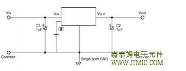
一,产品概述(General Description) 四.下载产品资料PDF文档 需要详细的PDF规格书请扫一扫微信联系我们,还可以获得免费样品以及技术支持! 五,产品封装图 (Package) 七,功能概述 |


-
项目
符号
条件
最小值
典型值
最大值
单位
输出电压*1
VOUT(E)
VIN =VOUT(S)+1.0 V, IOUT=30 mA
VOUT(S)
×0.98VOUT(S)
VOUT(S)
×1.02V
输出电流*2
IOUT
VIN≥2.5 V
300 *5
—
—
mA
输入输出压差
*3Vdrop
IOUT=50 mA
—
0.12
0.20
V
IOUT=100 mA
—
0.30
0.45
输入稳定度
DVOUT 1
DVIN ·VOUTVOUT(S)+0.5 V ≤VIN≤7 V
IOUT=30 mA—
0.10
0.20
%/V
负载稳定度
DVOUT2
VIN=VOUT(S)+1.0 V
1.0 mA ≤IOUT ≤100 mA—
50
100
mV
输出电压
温度系数*4DVOUT
DTa · VOUTVIN=VOUT(S)+1.0 V, IOUT=10 mA
-40°C ≤ Ta ≤85°C—
±100
—
ppm/℃
工作消耗电流
ISS1
VIN=VOUT(S)+1.0 V
—
50
μA
输入电压
VIN
——
1.8
—
5
V
纹波抑制率
|PSRR|
VIN=VOUT(S)+1.0 V,f=10 kHz
Vrip=0.5 Vrms, IOUT=50 mA—
60
—
dB
短路电流
Ishort
VIN=VOUT(S)+1.0 V,
ON/OFF 端子为 ON,VOUT=0 V—
60
—
mA
CE 最小高电平
VCEH
1.2
V
CE 最小低电平
VCEL
0.3
V
CE 为高电流
ICEH
VIN=VCE=VOUT(T)+1V
-0.1
0.1
μA
CE 为低电流
ICEL
VIN= VOUT(T)+1V ,VCE=VSS
-0.1
0.1
μA
-
八,相关产品
-
产品名称 工作电压(V) 输出电流(mA) 静态功耗(uA) 纹波抑制比(dB) 封装形式 CXLD6434 1.8-5.0 300 50 60@1KHz SOT-23-5 CXLD6435 2.0-7.0 300 70 70@10KHz SOT-23-5 CXLD6436 2.0-7.0 300 70 70@10KHz SOT-23-5,SOT-353 CXLD6437 2.0-7.0 300 60 70@1KHz SOT-89-3,SOT-23-3


