The CXSD62183 integrates two synchronous buck PWM controller and high/low side power MOSFETs to generate VPP and VDDQ, two sourcing and sinking LDO linear regulator to generate VTT and VTTREF. It provides a complete power supply for DDR4 memory system. It offers the lowest total solution cost in system where space is at a premium. The CXSD62183 provides excellent transient response and accurate DC voltage output in PFM Mode. In Pulse Frequency Mode (PFM), the CXSD62183 provides very high efficiency over light to heavy loads with loadingmodulated switching frequencies. The CXSD62183 has maximum power indicator function in order to prevent over load condition. The device also has single enable for VPP and VDDQ with JEDEC sequence implemented. Moreover, the CXSD62183 integrates SMBus controller to program VDDQ output voltage, VDDQ DAC voltage adjustment, VDDQ voltage slew rate setting, and VDDQ PWM converter frequency. The CXSD62183 is equipped with accurate current-limit, output under-voltage, output over-voltage and over-temperature protections. A Power-On- Reset function monitors the voltage on VCC prevents wrong operation during power on
-
"
目录
7.相关产品
产品概述 返回TOP
The CXSD62183 integrates two synchronous buck PWM controller and high/low side power MOSFETs to generate VPP and VDDQ, two sourcing and sinking LDO linear regulator to generate VTT and VTTREF. It provides a complete power supply for DDR4 memory system. It offers the lowest total solution cost in system where space is at a premium. The CXSD62183 provides excellent transient response and accurate DC voltage output in PFM Mode. In Pulse Frequency Mode (PFM), the CXSD62183 provides very high efficiency over light to heavy loads with loadingmodulated switching frequencies. The CXSD62183 has maximum power indicator function in order to prevent over load condition. The device also has single enable for VPP and VDDQ with JEDEC sequence implemented. Moreover, the CXSD62183 integrates SMBus controller to program VDDQ output voltage, VDDQ DAC voltage adjustment, VDDQ voltage slew rate setting, and VDDQ PWM converter frequency. The CXSD62183 is equipped with accurate current-limit, output under-voltage, output over-voltage and over-temperature protections. A Power-On- Reset function monitors the voltage on VCC prevents wrong operation during power on
产品特点 返回TOP
Provide 4 Independent Outputs for VPP, VDDQ, VTT LDO andVTTREFLDO VDDQ Converter
· High Input Voltages Range from 4.5V to 25V Input Power
· Provide 1.2V (DDR4) or Adjustable Output Voltage Max to 1.8V by SMBus Control - +1% Accuracy over Temperature
· HighEfficiencyPerformance up to 90%scale & Low Shutdown Current<1uA
· Integrated High_Side N-Channel MOSFET 20mW and Low_Side N-Channel MOSFET 7mW@ VCC=5V
· Integrated Bootstrap Forward P-CH MOSFET
· Built in Internal Soft-Start: 0.6ms(typ.) and SoftStop Functions for PWM Output
· Built In Automatic PFM/PWM Mode Selection
· Programmable Switching Frequency
· S3 and S5 Pins Control The Device in S0, S3 or S4/ S5 State
· Built In PMAX Signal for Total Power Indicator · Power Good Monitoring · 60% Under-Voltage Protection (UVP)
· 125% Over-Voltage Protection (OVP)
· Built in Fixed Valley Current Limit Protection
· Built In Thermal Shutdown Function
· VPP Converter
· Integrated High_Side P-Channel MOSFET 220mW and Low_Side N-Channel MOSFET 200mW @ VCC=5V
· Excellent Reference Voltage = 0.6V - +1% Load/Line Regulations over all TC range
· Fixed 1MHz switching Frequency
· Built in Internal Soft-Start: 0.35ms(typ.) and SoftStop Functions for PWM Output
· 60% Under-Voltage Protection (UVP)
· 125% Over-Voltage Protection (OVP)
· Built in Fixed Valley Current Limit Protection
· Built In Thermal Shutdown Function +0.75A LDO Section (VTT)
· Support Only 10mF MLCC for Stability on VTT LDO
· VTT and VTTREF Track at Halfthe VDDQ byinternal divider
· Built In 0.75A Source/Sink Capability on VTT LDO and 10mA Source/Sink Capability on VTTREF LDO
· Independent Current Limit Protection
· Thermal Shutdown Protection
· 4mmx4mm 26-pin package (TQFN-26)
· HalogenandLeadFreeAvailable (RoHSCompliant)
应用范围 返回TOP
· DDR3 and DDR4 Memory Power Supplies
· NB/MB/Tablet
技术规格书(产品PDF) 返回TOP
需要详细的PDF规格书请扫一扫微信联系我们,还可以获得免费样品以及技术支持!

产品封装图 返回TOP


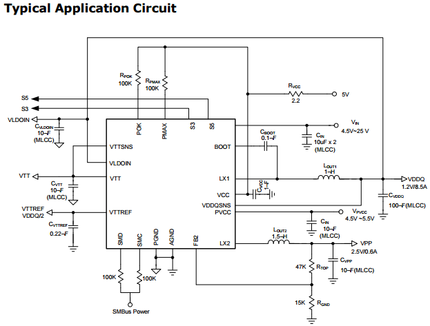
电路原理图 返回TOP
相关芯片选择指南 返回TOP 更多同类产品.......
|
Switching Regulator > Buck Converter |
|||||||||||
|
Part_No |
Package |
Architectu |
No.of PWM Outpu |
Drive Lout (A) |
Vin(V) |
Fmax Khz |
Vref (V) |
R-Top (milohm) |
R-Sync (milohm) |
Iq (No load) (uA) |
|
|
min |
max |
||||||||||
|
TQFN5x6-28 |
CM |
1 |
5 |
4.5 |
26 |
380 |
0.8 |
50 |
20 |
1000 |
|
|
SOP-8 |
CM |
1 |
2 |
4.5 |
26 |
380 |
0.8 |
100 |
1000 |
||
|
SOP-8P |
CM |
1 |
4 |
4.5 |
26 |
380 |
0.8 |
80 |
1000 |
||
|
SOT23-5|TSOT23-5 |
CM |
1 |
1 |
2.7 |
6 |
1500 |
0.6 |
280 |
250 |
25 |
|
|
SOT23-5 |
CM |
1 |
1 |
2.7 |
6 |
1500 |
0.6 |
280 |
250 |
||
|
SOP-8 |
CM |
1 |
3 |
4.3 |
14 |
500 |
0.8 |
70 |
70 |
500 |
|
|
SOP-8P |
CM |
1 |
3 |
4.3 |
14 |
500 |
0.8 |
55 |
45 |
500 |
|
|
TDFN3x3-10 |
3 |
2.6 |
5.5 |
2000 |
0.8 |
110 |
110 |
460 |
|||
|
TDFN3x3-10 |
CM |
2 |
1 |
2.7 |
6 |
1500 |
0.6 |
280 |
250 |
500 |
|
|
TDFN3x3-10 |
CM |
2 |
1 |
2.7 |
6 |
1500 |
0.6 |
280 |
250 |
||
|
TDFN2x2-6 |
CM |
1 |
1 |
2.7 |
6 |
1500 |
0.6 |
280 |
250 |
25 |
|
|
TDFN2x2-6 |
CM |
1 |
1 |
2.7 |
6 |
1500 |
0.6 |
280 |
250 |
||
|
TDFN3x3-12 |
CM |
2 |
1 |
2.7 |
6 |
1500 |
0.6 |
280 |
250 |
25 |
|
|
TDFN3x3-12 |
CM |
2 |
1 |
2.7 |
6 |
1500 |
0.6 |
280 |
250 |
||
|
TDFN 3x3 12 |
CM |
2 |
1 |
3 |
5.5 |
1500 |
0.6 |
280 |
250 |
30 |
|
|
TQFN3x3-20 |
CM |
3 |
2 |
2.9 |
5.5 |
1500 |
0.6 |
- |
- |
300 |
|
|
TDFN2x2-8 |
CM |
1 |
1 |
3.3 |
8 |
1500 |
0.6 |
280 |
250 |
25 |
|
|
SOP-8 |
CM |
1 |
2 |
4.5 |
24 |
340 |
0.925 |
110 |
110 |
1900 |
|
|
SOP-8P |
CM |
1 |
3 |
4.5 |
24 |
340 |
0.925 |
110 |
110 |
1900 |
|
|
SOP-8 |
CM |
1 |
2 |
4.5 |
24 |
340 |
|||||


