The CXSD62126 is a 3A synchronous-rectified Buck converter with integrated
70m Ω power MOSFETs. The CXSD62126, designed with a current-mode control
scheme,can convert wide input voltage of 4.3V to 14V to the output voltage
adjustable from 0.8V to VIN to provide excellent output voltage regulation.
For high efficiency over all load current range, the CXSD62126 is equipped
with an automatic Skip/PWM mode operation. At light load, the IC operates
in the Skip mode, which keeps a constant minimum inductor peak current,
to reduce switching losses. At heavy load, the IC works in PWM mode, which
inductor peak current is programmed by the COMP voltage, to provide high
efficiency and excel lent output voltage regulation.The CXSD62126 is also
equipped with power-on-reset,soft-start, soft-stop, and whole protections
(under-voltage,over-voltage, over-temperature, and current-limit) into a
single package. In shutdown mode, the supply current drops below 3μA.
This device, available in a 8-pin SOP-8 package, provides a very compact
system solution with minimal external components and PCB area.
-
"
目录
1.产品概述 2.产品特点
3.应用范围 4.下载产品资料PDF文档
5.产品封装图 6.电路原理图
7.功能概述 8.相关产品
一,产品概述(General Description)
The CXSD62126 is a 3A synchronous-rectified Buck converter with integrated
70m Ω power MOSFETs. The CXSD62126, designed with a current-mode control
scheme,can convert wide input voltage of 4.3V to 14V to the output voltage
adjustable from 0.8V to VIN to provide excellent output voltage regulation.
For high efficiency over all load current range, the CXSD62126 is equipped
with an automatic Skip/PWM mode operation. At light load, the IC operates
in the Skip mode, which keeps a constant minimum inductor peak current,
to reduce switching losses. At heavy load, the IC works in PWM mode, which
inductor peak current is programmed by the COMP voltage, to provide high
efficiency and excel lent output voltage regulation.The CXSD62126 is also
equipped with power-on-reset,soft-start, soft-stop, and whole protections
(under-voltage,over-voltage, over-temperature, and current-limit) into a
single package. In shutdown mode, the supply current drops below 3μA.
This device, available in a 8-pin SOP-8 package, provides a very compact
system solution with minimal external components and PCB area.
二.产品特点(Features)
Wide Input Voltage from 4.3V to 14V
Output Current up to 3A
Adjustable Output Voltage from 0.8V to V IN
- ±2% System Accuracy
70mΩ Integrated Power MOSFETs
High Efficiency up to 95%
- Automatic Skip/PWM Mode Operation
Current-Mode Operation
- Easy Feedback Compensation
- Stable with Low ESR Output Capacitors
- Fast Load/Line Transient Response
Power-On-Reset Monitoring
Fixed 500kHz Switching Frequency in PWM Mode
Built-In Digital Soft-Start and Soft-Stop
Current-Limit Protection with Frequency Foldback
123% Over-Voltage Protection
Hiccup-Mode 50% Under-Voltage Protection
Over-Temperature Protection
<3μA Quiescent Current in Shutdown Mode
Small SOP-8 Package
Lead Free and Green Devices Available
(RoHS Compliant)
三,应用范围 (Applications)
OLPC, UMPC
Notebook Computer
Handheld Portable Device
Step-Down Converters Requiring High Efficiency
and 3A Output Current
四.下载产品资料PDF文档
需要详细的PDF规格书请扫一扫微信联系我们,还可以获得免费样品以及技术支持!

五,产品封装图 (Package)

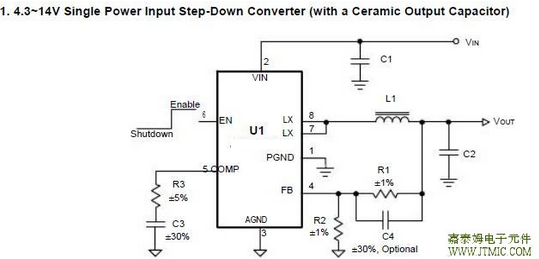
六.电路原理图
七,功能概述
Thermal Consideration
In most applications, the JTMA7104A does not dissipate much heat due to its high efficiency. But, in applications
where the JTMA7104A is running at high ambient tem perature with low supply voltage and high duty cycles, the
heat dissipated may exceed the maximum junction temperature of the part. If the junction temperature reaches
approximately 150°C, both power switches will be turned off and the SW node will become high impedance.
To avoid the JTMA7104A from exceeding the maximum junction temperature, the user will need to do some ther-
mal analysis. The goal of the thermal analysis is to deter mine whether the power dissipated exceeds the maxi-
mum junction temperature of the part. The power dissipated by the part is approximated:
PD ≅ IOUT2 x (RP-FET x D+RN-FET x (1-D))
The temperature rise is given by:
TR = (PD)(èJA)
Where PD is the power dissipated by the regulator, D is
duty cycle of main switch
D = VOUT/VIN
The èJA is the thermal resistance from the junction of the
die to the ambient temperature. The junction temperature,
TJ, is given by:
TJ = TA + TR
Where TA is the ambient temperature.
Layout Consideration
For all switching power supplies, the layout is an impor tant step in the design; especially at high peak currents
and switching frequencies. If the layout is not carefully done, the regulator might show noise problems and duty
cycle jitter.
1. The input capacitor should be placed close to the VIN and GND. Connecting the capacitor and VIN/GND with
short and wide trace without any via holes for good input voltage filtering. The distance between VIN/GND
to capacitor less than 2mm respectively is recommended.
2. To minimize copper trace connections that can inject noise into the system, the inductor should be placed
as close as possible to the SW pin to minimize the noise coupling into other circuits.
3. The output capacitor should be place closed to converter VOUT and GND.
4. Since the feedback pin and network is a high imped ance circuit the feedback network should be routed
away from the inductor. The feedback pin and feedback network should be shielded with a ground plane
or trace to minimize noise coupling into this circuit.
5. A star ground connection or ground plane minimizes ground shifts and noise is recommended.
八,相关产品 更多同类产品.......
|
Switching Regulator > Buck Converter |
|||||||||||
|
Part_No |
Package |
Architectu |
No.of PWM Outpu |
Drive Lout (A) |
Vin(V) |
Fmax Khz |
Vref (V) |
R-Top (milohm) |
R-Sync (milohm) |
Iq (No load) (uA) |
|
|
min |
max |
||||||||||
|
TQFN5x6-28 |
CM |
1 |
5 |
4.5 |
26 |
380 |
0.8 |
50 |
20 |
1000 |
|
|
SOP-8 |
CM |
1 |
2 |
4.5 |
26 |
380 |
0.8 |
100 |
1000 |
||
|
SOP-8P |
CM |
1 |
4 |
4.5 |
26 |
380 |
0.8 |
80 |
1000 |
||
|
SOT23-5|TSOT23-5 |
CM |
1 |
1 |
2.7 |
6 |
1500 |
0.6 |
280 |
250 |
25 |
|
|
SOT23-5 |
CM |
1 |
1 |
2.7 |
6 |
1500 |
0.6 |
280 |
250 |
||
|
SOP-8 |
CM |
1 |
3 |
4.3 |
14 |
500 |
0.8 |
70 |
70 |
500 |
|
|
SOP-8P |
CM |
1 |
3 |
4.3 |
14 |
500 |
0.8 |
55 |
45 |
500 |
|
|
TDFN3x3-10 |
3 |
2.6 |
5.5 |
2000 |
0.8 |
110 |
110 |
460 |
|||
|
TDFN3x3-10 |
CM |
2 |
1 |
2.7 |
6 |
1500 |
0.6 |
280 |
250 |
500 |
|
|
TDFN3x3-10 |
CM |
2 |
1 |
2.7 |
6 |
1500 |
0.6 |
280 |
250 |
||
|
TDFN2x2-6 |
CM |
1 |
1 |
2.7 |
6 |
1500 |
0.6 |
280 |
250 |
25 |
|
|
TDFN2x2-6 |
CM |
1 |
1 |
2.7 |
6 |
1500 |
0.6 |
280 |
250 |
||
|
TDFN3x3-12 |
CM |
2 |
1 |
2.7 |
6 |
1500 |
0.6 |
280 |
250 |
25 |
|
|
TDFN3x3-12 |
CM |
2 |
1 |
2.7 |
6 |
1500 |
0.6 |
280 |
250 |
||
|
TDFN 3x3 12 |
CM |
2 |
1 |
3 |
5.5 |
1500 |
0.6 |
280 |
250 |
30 |
|
|
TQFN3x3-20 |
CM |
3 |
2 |
2.9 |
5.5 |
1500 |
0.6 |
- |
- |
300 |
|
|
TDFN2x2-8 |
CM |
1 |
1 |
3.3 |
8 |
1500 |
0.6 |
280 |
250 |
25 |
|
|
SOP-8 |
CM |
1 |
2 |
4.5 |
24 |
340 |
0.925 |
110 |
110 |
1900 |
|
|
SOP-8P |
CM |
1 |
3 |
4.5 |
24 |
340 |
0.925 |
110 |
110 |
1900 |
|


