The CXSD62123 is a 2A, asynchronous, step-down con-verter with integrated
100mΩ P-channel MOSFET. The device, with current-mode control scheme, can
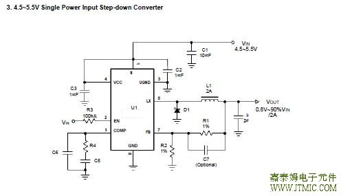
convert 4.5~26V input voltage to the output voltage adjustable from 0.8 to 90%
VIN to provide excellent output voltage regulation.
The CXSD62123 regulates the output voltage in automatic PSM/PWM mode
operation, depending on the output current, for high efficiency operation over light
to full load current. The CXSD62123 is also equipped with power-on-reset, soft-start, and whole protections (under-voltage,over- temperature, and current-limit)
into a single package.In shutdown mode, the supply current drops below 5μA.
This device, available in a 8-pin SOP-8 package, pro-vides a very compact
system solution with minimal exter-nal components.
-
"
|
目录 1.产品概述 2.产品特点 一,产品概述(General Description) VIN to provide excellent output voltage regulation. into a single package.In shutdown mode, the supply current drops below 5μA. This device, available in a 8-pin SOP-8 package, pro-vides a very compact system solution with minimal exter-nal components. 四.下载产品资料PDF文档 需要详细的PDF规格书请扫一扫微信联系我们,还可以获得免费样品以及技术支持! 五,产品封装图 (Package)
|


七,功能概述
Inductor Value Calculation
The operating frequency and inductor selection are interrelated in that higher operating frequencies permit the use of a smaller inductor for the same amount of inductorripple current. However, this is at the expense of efficiency
due to an increase in MOSFET gate charge losses. The equation (2) shows that the inductance value has a direct
effect on ripple current.Accepting larger values of ripple current allows the use of low inductances but results in
higher output voltage ripple and greater core losses. A reasonable starting point for setting ripple current is
∆I ≤ 0.4. IOUT(MAX). Remember, the maximum ripple current occurs at the maximum input voltage.
Output Diode Selection
The Schottky diode carries load current during the offtime. Therefore, the average diode current is dependent
on the P-channel power MOSFET duty cycle. At high input voltages, the diode conducts most of the time. As VIN ap-proaches VOUT, the diode conducts only a small fraction of the time. The most stressful condition for the diode is when the output is short-circuited. Therefore, it is important to adequately specify the diode peak current and av-
erage power dissipation so as not to exceed the diode ratings.
In high power switching regulator, a correct layout is important to ensure proper operation of the regulator. In
general, interconnecting impedance should be minimized by using short and wide printed circuit traces. Signal and
power grounds are to be kept separating and finally c om bined using ground plane construction or
single point grounding. Figure 2 illustrates the layout,with bold lines indicating high current paths. Components along the bold lines should be placed close together.
Below is a checklist for your layout:
pedances should be minimized by using wide and short printed circuit traces.
3. Keep the sensitive small signal nodes (FB, COMP)away from switching nodes (LX or others) on the PCB.
Therefore, place the feedback divider and the feedback compensation network close to the IC to avoid switch-
ing noise. Connect the ground of feedback divider directly to the GND pin of the IC using a dedicated
ground trace.
4. The VCC decoupling capacitor should be right next to the VCC and GND pins. Capacitor C2 should be
connected as close to the VIN and UGND pins as possible.
5. Place the decoupling ceramic capacitor C1 near the VIN as close as possible. The bulk capacitors C8 are
also placed near VIN. Use a wide power ground plane to connect the C1, C8, C4, and Schottky diode to pro-
vide a low impedance path between the components for large and high slew rate current.
八,相关产品 更多同类产品.......
|
Switching Regulator > Buck Converter |
|||||||||||
|
Part_No |
Package |
Architectu |
No.of PWM Outpu |
Drive Lout (A) |
Vin(V) |
Fmax Khz |
Vref (V) |
R-Top (milohm) |
R-Sync (milohm) |
Iq (No load) (uA) |
|
|
min |
max |
||||||||||
|
TQFN5x6-28 |
CM |
1 |
5 |
4.5 |
26 |
380 |
0.8 |
50 |
20 |
1000 |
|
|
SOP-8 |
CM |
1 |
2 |
4.5 |
26 |
380 |
0.8 |
100 |
1000 |
||
|
SOP-8P |
CM |
1 |
4 |
4.5 |
26 |
380 |
0.8 |
80 |
1000 |
||
|
SOT23-5|TSOT23-5 |
CM |
1 |
1 |
2.7 |
6 |
1500 |
0.6 |
280 |
250 |
25 |
|
|
SOT23-5 |
CM |
1 |
1 |
2.7 |
6 |
1500 |
0.6 |
280 |
250 |
||
|
SOP-8 |
CM |
1 |
3 |
4.3 |
14 |
500 |
0.8 |
70 |
70 |
500 |
|
|
SOP-8P |
CM |
1 |
3 |
4.3 |
14 |
500 |
0.8 |
55 |
45 |
500 |
|
|
TDFN3x3-10 |
3 |
2.6 |
5.5 |
2000 |
0.8 |
110 |
110 |
460 |
|||
|
TDFN3x3-10 |
CM |
2 |
1 |
2.7 |
6 |
1500 |
0.6 |
280 |
250 |
500 |
|
|
TDFN3x3-10 |
CM |
2 |
1 |
2.7 |
6 |
1500 |
0.6 |
280 |
250 |
||
|
TDFN2x2-6 |
CM |
1 |
1 |
2.7 |
6 |
1500 |
0.6 |
280 |
250 |
25 |
|
|
TDFN2x2-6 |
CM |
1 |
1 |
2.7 |
6 |
1500 |
0.6 |
280 |
250 |
||
|
TDFN3x3-12 |
CM |
2 |
1 |
2.7 |
6 |
1500 |
0.6 |
280 |
250 |
25 |
|
|
TDFN3x3-12 |
CM |
2 |
1 |
2.7 |
6 |
1500 |
0.6 |
280 |
250 |
||
|
TDFN 3x3 12 |
CM |
2 |
1 |
3 |
5.5 |
1500 |
0.6 |
280 |
250 |
30 |
|
|
TQFN3x3-20 |
CM |
3 |
2 |
2.9 |
5.5 |
1500 |
0.6 |
- |
- |
300 |
|
|
TDFN2x2-8 |
CM |
1 |
1 |
3.3 |
8 |
1500 |
0.6 |
280 |
250 |
25 |
|
|
SOP-8 |
CM |
1 |
2 |
4.5 |
24 |
340 |
0.925 |
110 |
110 |
1900 |
|
|
SOP-8P |
CM |
1 |
3 |
4.5 |
24 |
340 |
0.925 |
110 |
110 |
1900 |
|


