The CXSD6295 is a voltage mode, fixed 300kHz switching frequency, synchronous buck converter. The CXSD6295 allows wide input voltage that is either a single 5~12V or two supply voltage(s) for various applications. A power-on-reset (POR) circuit monitors the VCC supply voltage to prevent wrong logic controls. A built-in soft-start circuit prevents the output voltages from overshoot as well as limits the input current. An internal 0.8V tempera ture-compensated reference voltage with high accuracy is designed to meet the requirement of low output voltage applications. The CXSD6295 provides excellent out put voltage regulations against load current variation.The controller’s over-current protection monitors the out-put current by using the voltage drop across the RDS(ON) of low-side MOSFET, eliminating the need for a current sensing resistor that features high efficiency and low cost. In addition, the CXSD6295 also integrates excellent protection functions: The over-voltage protection (OVP) , under voltage protection (UVP). OVP circuit which monitors the FB voltage to prevent the PWM output from over-voltage,and UVP circuit which monitors the FB voltage to prevent the PWM output from under-voltage or short-circuit.
-
"
目录
1.产品概述 2.产品特点
3.应用范围 4.下载产品资料PDF文档
5.产品封装图 6.电路原理图
7.功能概述 8.相关产品
一,产品概述(General Description)
The CXSD6295 is a voltage mode, fixed 300kHz switching frequency, synchronous buck converter. The CXSD6295 allows wide input voltage that is either a single 5~12V or two supply voltage(s) for various applications. A power-on-reset (POR) circuit monitors the VCC supply voltage to prevent wrong logic controls. A built-in soft-start circuit prevents the output voltages from overshoot as well as limits the input current. An internal 0.8V tempera ture-compensated reference voltage with high accuracy is designed to meet the requirement of low output voltage applications. The CXSD6295 provides excellent out put voltage regulations against load current variation.The controller’s over-current protection monitors the out-put current by using the voltage drop across the RDS(ON) of low-side MOSFET, eliminating the need for a current sensing resistor that features high efficiency and low cost. In addition, the CXSD6295 also integrates excellent protection functions: The over-voltage protection (OVP) , under voltage protection (UVP). OVP circuit which monitors the FB voltage to prevent the PWM output from over-voltage,and UVP circuit which monitors the FB voltage to prevent the PWM output from under-voltage or short-circuit.
The CXSD6295 is available in SOP-8P and TDFN3x3-10 packages.
二.产品特点(Features)
1.)Wide 5V to 12V Supply Voltage
2.)Power-On-Reset Monitoring on VCC
3.)Excellent Output Voltage Regulations
0.8V Internal Reference
±1% Over-Temperature Range
4.)Integrated Soft-Start
5.)Voltage Mode PWM Operation with External Compensation
6.)Up to 90% Duty Ratio for Fast Transient Response
7.)Constant Switching Frequency 300kHz ±10%
8.)9V Driver Voltage for BOOT Supply with Internal Bootstrap Diode
9.)Drive Dual Low Cost N-MOSFETs with Adaptive Dead-Time Control
10.)50% Under-Voltage Protection
11.)125% Over-Voltage Protection
12.)Adjustable Over-Current Protection Threshold
Using the RDS(ON) of Low-Side MOSFET
13.)Shutdown Control by COMP
14.)Power Good Monitoring (TDFN-10 3mmx3mm Package Only)
SOP-8P and TDFN3x3-10 Packages
15.)Lead Free and Green Devices Available (RoHS Compliant)
三,应用范围 (Applications)
Graphic Cards
DSL, Switch HUB
Wireless Lan
Notebook Computer
Mother Board
LCD Monitor/TV
四.下载产品资料PDF文档
需要详细的PDF规格书请扫一扫微信联系我们,还可以获得免费样品以及技术支持!

五,产品封装图 (Package)


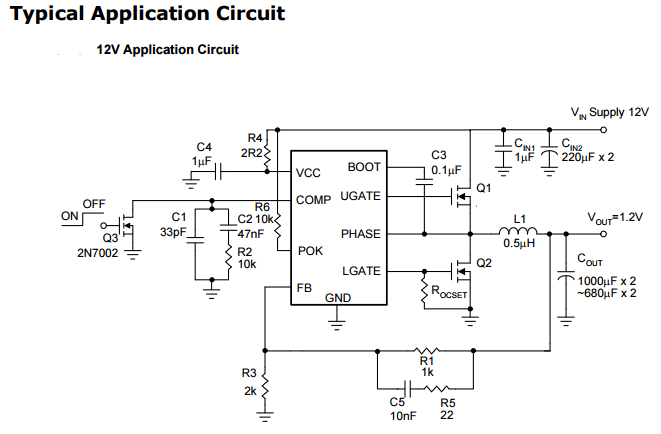
六.电路原理图

七,功能概述
Output Capacitor Selection
The selection of COUT is determined by the required effec-tive series resistance (ESR) and voltage
rating rather than the actual capacitance requirement. Therefore, selecting high performance low ESR
capacitors is intended for switching regulator applications. In some applications,multiple capacitors have
to be paralleled to achieve the desired ESR value. If tantalum capacitors are used, make sure they are
surge tested by the manufactures. If in doubt,consult the capacitors manufacturer.
Input Capacitor Selection
The input capacitor is chosen based on the voltage rat-ing and the RMS current rating. For reliable operation,
select the capacitor voltage rating to be at least 1.3 times higher than the maximum input voltage. The maximum
RMS current rating requirement is approximately IOUT/2 where IOUT is the load current. During power up, the
input capacitors have to handle large amount of surge current.If tantalum capacitors are used, make sure they
are surge tested by the manufactures. If in doubt, consult the ca-pacitors manufacturer.For high frequency
decoupling, a ceramic capacitor be-tween 0.1μF to 1μF can connect between VCC and ground pin.
Inductor Selection
The inductance of the inductor is determined by the out-put voltage requirement. The larger the inductance,
the lower the inductor’s current ripple. This will translate into lower output ripple voltage. The ripple current
and ripple voltage can be approximated by:
× OUT
FSW × L VIN
where Fs is the switching frequency of the regulator.
∆VOUT = IRIPPLE x ESR
A tradeoff exists between the inductor’s ripple current and the regulator load transient response time. A smaller
in-ductor will give the regulator a faster load transient re-sponse at the expense of higher ripple current and vice
versa. The maximum ripple current occurs at the maxi-mum input voltage. A good starting point is to choose the
ripple current to be approximately 30% of the maximum output current.Once the inductance value has been chosen, selecting an inductor is capable of carrying the required peak cur-rent without going into saturation. In some types of inductors, especially core that is make of ferrite, the ripple current will increase abruptly when it saturates. This will result in a larger output ripple voltage.
Compensation
The output LC filter of a step down converter introduces a double pole, which contributes with -40dB/decade gain
slope and 180 degrees phase shift in the control loop. A compensation network between COMP pin and ground
should be added. The simplest loop compensation net-work is shown in Figure 5.
The output LC filter consists of the output inductor and output capacitors. The transfer function of the LC filter is
given by:
The FLC is the double poles of the LC filter, and FESR is the zero introduced by the ESR of the output capacitor.
八,相关产品 更多同类产品......
|
Switching Regulator > Buck Controller |
||||||||||
|
Part_No |
Package |
Archi tectu |
Phase |
No.of PWM Output |
Output Current (A) |
Input Voltage (V) |
Reference Voltage (V) |
Bias Voltage (V) |
Quiescent Current (uA) |
|
|
min |
max |
|||||||||
|
SOP-14 QSOP-16 QFN4x4-16 |
VM |
1 |
1 |
30 |
2.9 |
13.2 |
0.9 |
12 |
8000 |
|
|
SOP-8 |
VM |
1 |
1 |
20 |
2.9 |
13.2 |
0.8 |
12 |
5000 |
|
|
SOP-8 |
VM |
1 |
1 |
20 |
2.9 |
13.2 |
0.8 |
12 |
5000 |
|
|
QFN4x4-24 |
VM |
2 |
1 |
60 |
3.1 |
13.2 |
0.6 |
12 |
5000 |
|
|
SOP-8 |
VM |
1 |
1 |
20 |
2.2 |
13.2 |
0.8 |
5~12 |
2100 |
|
|
SOP-8 |
VM |
1 |
1 |
20 |
2.2 |
13.2 |
0.8 |
5~12 |
2100 |
|
|
SOP8|TSSOP8 |
VM |
1 |
1 |
5 |
5 |
13.2 |
1.25|0.8 |
5~12 |
3000 |
|
|
SOP-8 |
VM |
1 |
1 |
10 |
3.3 |
5.5 |
0.8 |
5 |
2100 |
|
|
SOP-14 |
VM |
1 |
1 |
10 |
5 |
13.2 |
0.8 |
12 |
2000 |
|
|
TSSOP-24 |QFN5x5-32 |
VM |
1 |
2 |
20 |
5 |
13.2 |
0.6 |
5~12 |
4000 |
|
|
SOP14 QSOP16 QFN-16 |
VM |
1 |
1 |
30 |
2.9 |
13.2 |
0.9 |
12 |
4000 |
|
|
SOP-14 |
VM |
1 |
1 |
30 |
2.2 |
13.2 |
0.6 |
12 |
5000 |
|
|
SOP-14 |
VM |
1 |
1 |
30 |
2.2 |
13.2 |
0.6 |
12 |
5000 |
|
|
SOP-14 |
VM |
1 |
1 |
25 |
2.2 |
13.2 |
0.8 |
12 |
5000 |
|
|
LQFP7x7 48 TQFN7x7-48 |
VM |
1 |
6 |
0.015 |
1.4 |
6.5 |
- |
5 |
1800 |
|
|
TSSOP-24P |
VM |
1 |
2 |
20 |
2.97 |
5.5 |
0.8 |
5~12 |
5000 |
|
|
SOP-14 |
VM |
1 |
1 |
10 |
5 |
13.2 |
0.8 |
12 |
3000 |
|
|
SOP-8-P|DIP-8 |
VM |
1 |
1 |
30 |
2.9 |
13.2 |
1.2 |
12 |
3000 |
|
|
SSOP28 QFN4x4-24 |
VM |
1 |
||||||||


