The CXSD6286 integrates PWM and linear controller, as well as the monitoring and protection functions into a single package. The synchronous PWM controller which drives dual N-channel MOSFETs, which provides one controlled power outputs with under-voltage and over-current protections. Linear controller drives an external N-channel MOSFET with under-voltage protection.
CXSD6286 provides excellent regulation for output load variation. An internal 0.8V temperature-compensated ref-erence voltage is designed to meet the arious low out-put voltage applications. CXSD6286 includes a 250kHz free-running triangle-wave oscillator that is adjustable from 70kHz to 800kHz.A power-on-reset (POR) circuit limits the VCC minimum opearting supply voltage to assure the controller working well. Over current protection is achieved by monitoring the voltage drop across the low side MOSFET, eliminat-ing the need for a current sensing resistor and short cir-cuit condition is detected through the FB pin. The over-current protection triggers the soft-start function until the fault events be removed, but Under-voltage protection will shutdown IC directly.Pull the COMP pin below 0.4V will shutdown the controller,and both gate drive signals will be low
-
"
目录
1.产品概述 2.产品特点
3.应用范围 4.下载产品资料PDF文档
5.产品封装图 6.电路原理图
7.功能概述 8.相关产品
一,产品概述(General Description)
The CXSD6286 integrates PWM and linear controller, as well as the monitoring and protection functions into a single package. The synchronous PWM controller which drives dual N-channel MOSFETs, which provides one controlled power outputs with under-voltage and over-current protections. Linear controller drives an external N-channel MOSFET with under-voltage protection.
CXSD6286 provides excellent regulation for output load variation. An internal 0.8V temperature-compensated ref-erence voltage is designed to meet the arious low out-put voltage applications. CXSD6286 includes a 250kHz free-running triangle-wave oscillator that is adjustable from 70kHz to 800kHz.A power-on-reset (POR) circuit limits the VCC minimum opearting supply voltage to assure the controller working well. Over current protection is achieved by monitoring the voltage drop across the low side MOSFET, eliminat-ing the need for a current sensing resistor and short cir-cuit condition is detected through the FB pin. The over-current protection triggers the soft-start function until the fault events be removed, but Under-voltage protection will shutdown IC directly.Pull the COMP pin below 0.4V will shutdown the controller,and both gate drive signals will be low
二.产品特点(Features)
1.)Provide Two Regulated Voltages
- Synchronous Rectified Buck PWM Controller
- Linear Controller
2.)Fast Transient Response
- 0~85% Duty Ratio
3.)Excellent Output Voltage Regulation
- 0.8V Internal Reference
- ±1% Over Line Voltage and Temperature
4.)Over Current Protection
- Sense Low-Side MOSFET’s RDS(ON)
5.)Under Voltage Lockout
6.)Small Converter Size
- 250kHz Free-Running Oscillator
- Programmable From 70kHz to 800kHz
7.)14-Lead SOIC Package
8.)Lead Free and Green Devices Available
(RoHS Compliant)
三,应用范围 (Applications)
Graphic Cards
Memory Power Supplies
DSL or Cable MODEMs
Set Top Boxes
Low-Voltage Distributed Power Supplies
四.下载产品资料PDF文档
需要详细的PDF规格书请扫一扫微信联系我们,还可以获得免费样品以及技术支持!

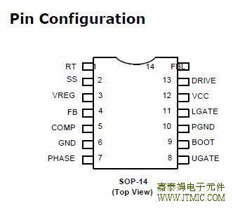
五,产品封装图 (Package)
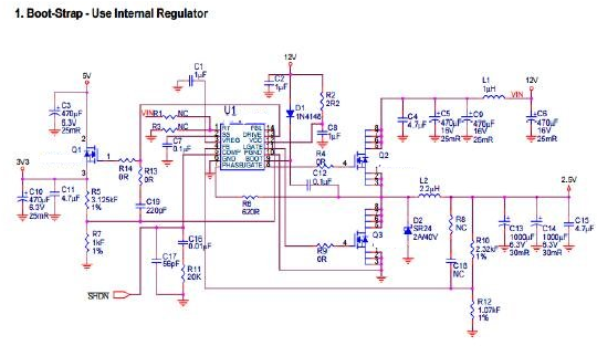
六.电路原理图

七,功能概述
MOSFET Selection
The selection of the N-channel power MOSFETs is deter-mined by the RDS(ON), reverse transfer
capacitance (CRSS),and maximum output current requirement.The losses in the MOSFETs have two
components: conduction loss and transition loss. For the upper and lower MOSFET, the losses are
approximately given by the following equations:
PUPPER = Iout (1+ TC)(RDS(ON))D + (0.5)(Iout)(VIN)(tsw)FS
where IOUT is the load current
TC is the temperature dependency of RDS(ON)
FS is the switching frequency
tsw is the switching interval
D is the duty cycle
Note that both MOSFETs have conduction losses while the upper MOSFET include an additional transition
loss.The switching internal, tsw, is the function of the reverse transfer capacitance CRSS. Figure 7 illustrates
the switch-ing waveform internal of the MOSFET.The (1+TC) term factors in the temperature dependency
of the RDS(ON) and can be extracted from the “RDS(ON) vs Tem-perature” curve of the power MOSFET.
Linear Regulator Input/Output Capacitor Selection
The input capacitor is chosen based on its voltage rating.Under load transient condition, the input capacitor will
momentarily supply the required transient current. A 1μF ceramic capacitor will be sufficient in most applications.
The output capacitor for the linear regulator is chosen to minimize any droop during load transient condition. In
addition, the capacitor is chosen based on its voltage rating.
Linear Regulator MOSFET Selection
The maximum DRIVE voltage is determined by the VCC.Since this pin drives an external N-channel MOSFET,
the maximum output voltage of the linear regulator is depen-dent upon the VGS.
VOUT2MAX = VCC- VGS
Another criteria is its efficiency of heat removal. The power dissipated by the MOSFET is given by:
Pdiss = Iout * (VIN - VOUT2)
where Iout is the maximum load current
Vout2 is the nominal output voltage In some applications, heatsink may be required to help
maintain the junction temperature of the MOSFET below its maximum rating.
Layout Consideration
In high power switching regulator, a correct layout is im-portant to ensure proper operation of the regulator. In
general, interconnecting impedances should be mini-mized by using short and wide printed circuit traces. Sig-
nal and power grounds are to be kept separate and finally combined using ground plane construction or single point grounding. Figure 8 illustrates the layout, with bold lines indicating high current paths. Components along the bold lines should be placed close together. Below is a check-list for your layout:
· Keep the switching nodes (UGATE, LGATE, and PHASE)away from sensitive small signal nodes since these
nodes are fast moving signals. Therefore, keep traces to these nodes as short as possible.
· The ground return of CIN must return to the combine COUT (-) terminal.
八,相关产品 更多同类产品......
|
Switching Regulator > Buck Controller |
||||||||||
|
Part_No |
Package |
Archi tectu |
Phase |
No.of PWM Output |
Output Current (A) |
Input Voltage (V) |
Reference Voltage (V) |
Bias Voltage (V) |
Quiescent Current (uA) |
|
|
min |
max |
|||||||||
|
SOP-14 QSOP-16 QFN4x4-16 |
VM |
1 |
1 |
30 |
2.9 |
13.2 |
0.9 |
12 |
8000 |
|
|
SOP-8 |
VM |
1 |
1 |
20 |
2.9 |
13.2 |
0.8 |
12 |
5000 |
|
|
SOP-8 |
VM |
1 |
1 |
20 |
2.9 |
13.2 |
0.8 |
12 |
5000 |
|
|
QFN4x4-24 |
VM |
2 |
1 |
60 |
3.1 |
13.2 |
0.6 |
12 |
5000 |
|
|
SOP-8 |
VM |
1 |
1 |
20 |
2.2 |
13.2 |
0.8 |
5~12 |
2100 |
|
|
SOP-8 |
VM |
1 |
1 |
20 |
2.2 |
13.2 |
0.8 |
5~12 |
2100 |
|
|
SOP8|TSSOP8 |
VM |
1 |
1 |
5 |
5 |
13.2 |
1.25|0.8 |
5~12 |
3000 |
|
|
SOP-8 |
VM |
1 |
1 |
10 |
3.3 |
5.5 |
0.8 |
5 |
2100 |
|
|
SOP-14 |
VM |
1 |
1 |
10 |
5 |
13.2 |
0.8 |
12 |
2000 |
|
|
TSSOP-24 |QFN5x5-32 |
VM |
1 |
2 |
20 |
5 |
13.2 |
0.6 |
5~12 |
4000 |
|
|
SOP14 QSOP16 QFN-16 |
VM |
1 |
1 |
30 |
2.9 |
13.2 |
0.9 |
12 |
4000 |
|
|
SOP-14 |
VM |
1 |
1 |
30 |
2.2 |
13.2 |
0.6 |
12 |
5000 |
|
|
SOP-14 |
VM |
1 |
1 |
30 |
2.2 |
13.2 |
0.6 |
12 |
5000 |
|
|
SOP-14 |
VM |
1 |
1 |
25 |
2.2 |
13.2 |
0.8 |
12 |
5000 |
|
|
LQFP7x7 48 TQFN7x7-48 |
VM |
1 |
6 |
0.015 |
1.4 |
6.5 |
- |
5 |
1800 |
|
|
TSSOP-24P |
VM |
1 |
2 |
20 |
2.97 |
5.5 |
0.8 |
5~12 |
5000 |
|
|
SOP-14 |
VM |
1 |
1 |
10 |
5 |
13.2 |
0.8 |
12 |
3000 |
|
|
SOP-8-P|DIP-8 |
VM |
1 |
1 |
30 |
2.9 |
13.2 |
1.2 |
12 |
3000 |
|
|
SSOP28 QFN4x4-24 |
VM |
1 |
2 |
20 |
5 |
24 |
0.9 |
5 |
1200 |
|
|
|
||||||||||


