The CXSD62361/A is intended for DDR/SSTL-2, DDRII/SSTL-18 and DDRIII memory systems. It integrates a synchronous buck PWM controller with a 3-A sink-source linear regulator and buffered reference. The PWM controller uses constant on-time control scheme to handle wide input/output voltage ratios with ease and provides 100ns “instant-on” response to load transients while maintaining a relatively constant switching frequency. The CXSD62361/A achieves high efficiency at a reduced cost by eliminating the current-sense resistor found in traditional current-mode PWMs. Efficiency is further enhanced by an ability to drive very large synchronous rectifier MOSFETs. Single-stage buck conversion allows these devices to directly step down high-voltage batteries for the highest possible efficiency. The 3A sink/source tracking termination regulator is specifically designed for low-cost/ low-external component count systems. The regulator contains a high speed operational amplifier that provides fast load transient response with only 20μF (2x10μF) of ceramic output capacitance. The CXSD62361/A supports remote sensing functions and all features required to power the DDR /DDRII /DDRIII VTT bus termination according to the JEDEC specification
-
"
目录
7.相关产品
产品概述 返回TOP
and VTTREF in S5 (Shutdown). The CXSD62361/A provides OVP, UVP, over The CXSD62361/A is intended for DDR/SSTL-2, DDRII/SSTL-18 and DDRIII memory systems. It integrates a synchronous buck PWM controller with a 3-A sink-source linear regulator and buffered reference. The PWM controller uses constant on-time control scheme to handle wide input/output voltage ratios with ease and provides 100ns “instant-on” response to load transients while maintaining a relatively constant switching frequency. The CXSD62361/A achieves high efficiency at a reduced cost by eliminating the current-sense resistor found in traditional current-mode PWMs. Efficiency is further enhanced by an ability to drive very large synchronous rectifier MOSFETs. Single-stage buck conversion allows these devices to directly step down high-voltage batteries for the highest possible efficiency. The 3A sink/source tracking termination regulator is specifically designed for low-cost/ low-external component count systems. The regulator contains a high speed operational amplifier that provides fast load transient response with only 20μF (2x10μF) of ceramic output capacitance. The CXSD62361/A supports remote sensing functions and all features required to power the DDR /DDRII /DDRIII VTT bus termination according to the JEDEC specification. In addition, the CXSD62361/A includes integrated sleep-state controls placing VTT in High-Z in S3 (suspend to RAM) and soft-off for VTT current and thermal shutdown protection functions and is available in a 20-pin 3X3 TQFN package and 24-pin 4X4 TQFN includes over voltage protection.
产品特点 返回TOP
•Synchronous Buck Controller (VDDQ)
„ Ultra-High Efficiency
„ No Current-Sense Resistor (Lossless ILIMIT)
„ Quasi-PWM with 100ns Load-Step Response
„ 1.8V(DDRII) /1.5V(DDRIII) Fixed or Adjustable to 2.5V(DDR) or 0.75V to 3.6V Adjustable Output Range
„ 2V to 24V Battery Input Range
„ 400kHz Switching Frequency
„ OVP & UVP of VDDQ Output
„ Drives Large Synchronous-Rectifier FETs
„ Power-Good Indicator
•3-A LDO (VTT), Buffered Reference (VTTREF)
„ Support DDR (1.25 VTT) , DDR II (0.9 VTT) and DDRIII(0.75 VTT) Requirements
„ VLDOIN Voltage Range: 1.2V to 3.6V
„ Requires Only 20μF Ceramic VTT Output Capacitance
„ Supports High-Z in S3 and Soft-Off in S5
„ Integrated Divider Tracks 1/2 VDDQSNS for Both VTT and VTTREF „ Remote Sensing (VTTSNS)
„ ±20mV Accuracy for VTT and VTTREF
„ 10mA Buffered Reference (VTTREF)
„ Built-In Soft-Start to Reduce the VLDOIN Surging Current
„ Over Current Protection of VTT Output
„ Thermal Shutdown Protection
应用范围 返回TOP
„ Notebook Computers
„ CPU Core Supply
„ Chipset/RAM Supply as Low as 0.75V
„ 1.8V and 2.5V I/O Supply
技术规格书(产品PDF) 返回TOP
需要详细的PDF规格书请扫一扫微信联系我们,还可以获得免费样品以及技术支持!

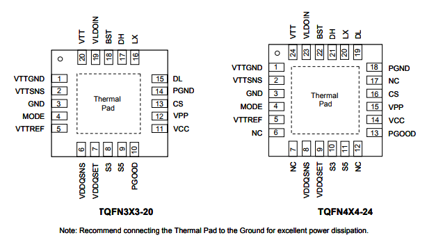
产品封装图 返回TOP
电路原理图 返回TOP
a
相关芯片选择指南 返回TOP 更多同类产品......
|
Synchronous (Quasi-PWM) Step Down Controller |
|||||||
|
Part NO. |
Vin(V) min. |
Vin(V) max. |
VOUT (V) |
FSW (k Hz) |
FB (V) |
Note |
Package |
|
3 |
28 |
0.7~1.8 |
300/400 |
0.8 |
EN, SS, PGOOD, OVP, UVP, OCP, VTTREF, Built-in BST diode, DDR1/2/3/3L, 2A LDO for VTT |
TQFN3X3-20 |
|
|
4.5 |
28 |
0.7~2.6 |
ADJ |
0.7 |
EN, PGOOD, OVP, UVP, OCP, VOUT Adjustable,1.5ms VOUT Servo Soft Start, 4700ppm/°C RON Coefficient |
TDFN3X3-10 |
|
|
4.5 |
28 |
0.5~3.3 |
ADJ |
0.5 |
EN, PGOOD, OVP, UVP, OCP, VOUT Adjustable, 1.5ms VOUT Servo Soft Start, 4700ppm/°C RON Coefficient |
TQFN2X2-12 |
|
|
4.5 |
24 |
0.75~3.6 |
ADJ |
0.75 |
EN, SS, PGOOD, OVP, UVP, OCP, Built-in BST diode |
TQFN3X3-16 |
|
|
4.5 |
24 |
0.75~3.6 |
ADJ |
0.75 |
EN, SS, PGOOD, OVP, UVP, OCP, Built-in BST diode |
TQFN3X3-16 |
|
|
4.5 |
24 |
0.75~3.6 |
ADJ |
0.75 |
EN, SS, PGOOD, OVP, UVP, OCP, Built-in BST diode |
TQFN3X3-16/TQFN3.5X3.5-14 |
|
|
2 |
24 |
0.75~3.6 |
400/ADJ |
0.75 |
EN, SS, PGOOD, OVP, UVP, OCP, VTTREF, Built-in BST diode, DDR1/2/3/3L, 3A/2A LDO for VTT |
TQFN4X4-24/TQFN3X3-20 |
|
|
4.5 |
24 |
0.75~3.6 |
ADJ |
0.75 |
EN, PGOOD, OVP, UVP, OCP, Built-in BST diode, SS, G0 & G1 Controls VOUT |
TQFN3X3-16 |
|