The CXSD6261 is a 180 KHz fixed frequency PWM buck (step-down)
DC/DC converter,capable of driving a 8A load with high efficiency, low ripple
and excellent line and load regulation.Requiring a minimum number
of external components, the regulator is simple to use and include internal
frequency compensation and a fixed-frequency oscillator.
The PWM control circuit is able to adjust the duty ratio linearly from
0 to 100%.An over current protection function is built inside.When
short protection function happens, the operation frequency
will be reduced from 180KHz to 48KHz. An internal compensation
block is built in to minimize external component count.
-
"
目录
1.产品概述 2.产品特点 3.应用范围 4.技术规格书下载(产品PDF文档)
5.产品封装图 6.电路原理图 7.功能概述 8.相关产品
一,产品概述(General Description) ![]()
The CXSD6261 is a 180 KHz fixed frequency PWM buck (step-down)
DC/DC converter,capable of driving a 8A load with high efficiency, low ripple
and excellent line and load regulation.Requiring a minimum number
of external components, the regulator is simple to use and include internal
frequency compensation and a fixed-frequency oscillator.
The PWM control circuit is able to adjust the duty ratio linearly from
0 to 100%.An over current protection function is built inside.When
short protection function happens, the operation frequency
will be reduced from 180KHz to 48KHz. An internal compensation
block is built in to minimize external component count.
二.产品特点(Features)![]()
Wide 8V to 40V Input Voltage Range
Output Adjustable from 1.25V to 36V
Maximum Duty Cycle 100%
Minimum Drop Out 0.3V
Fixed 180KHz Switching Frequency
8A Constant Output Current Capability
Internal Optimize Power MOSFET
High efficiency up to 96%
Excellent line and load regulation
Built in thermal shutdown function
Built in current limit function
Built in output short protection function
Built in input over voltage protection
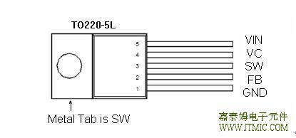
Available in TO220-5L package
三,应用范围 (Applications)![]()
LCD Monitor and LCD TV
Portable instrument power supply
Telecom / Networking Equipment
四.技术规格书下载(产品PDF)![]()
需要详细的PDF规格书请扫一扫微信联系我们,还可以获得免费样品以及技术支持!

五,产品封装图 (Package)![]()
|
Pin Number |
Pin Name |
Description |
|
1 |
GND |
Ground Pin. Care must be taken in layout. This pin should be |
|
2 |
FB |
Feedback Pin (FB). Through an external resistor divider |
|
3 |
SW |
Power Switch Output Pin (SW). SW is the switch node that |
|
4 |
VC |
Internal Voltage Regulator Bypass Capacity. In typical system |
|
5 |
VIN |
Supply Voltage Input Pin. CXSD6261 operates from a 8V to 40V |
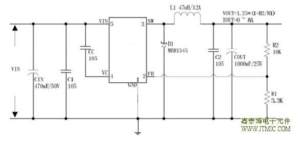
六.电路原理图![]()
七,功能概述![]()
|
Parameter |
Symbol |
Value |
Unit |
|
Input Voltage |
Vin |
-0.3 to 45 |
V |
|
Feedback Pin Voltage |
VFB |
-0.3 to Vin |
V |
|
Output Switch Pin Voltage |
VOutput |
-0.3 to Vin |
V |
|
Power Dissipation |
PD |
Internally limited |
mW |
|
Thermal Resistance (TO220-5L) |
RJA |
30 |
oC/W |
|
Operating Junction Temperature |
TJ |
-40 to 125 |
oC |
|
Storage Temperature |
TSTG |
-65 to 150 |
oC |
|
Lead Temperature (Soldering, 10 sec) |
TLEAD |
260 |
oC |
|
ESD (HBM) |
>2000 |
V |
八,相关芯片选择指南![]()
|
降压型直流电源变换器芯片(大功率型) |
|||||
|
产品型号 |
输入电压 |
开关电流 |
开关频率 |
电压版本 |
封装类型 |
|
5V ~ 32V |
4A |
300KHz |
Adj (0.8V) |
TO252-5L |
|
|
5V ~ 32V |
5A |
300KHz |
Adj (0.8V) |
TO263-5L |
|
|
8V ~ 36V |
4A |
180KHz |
Adj (1.25V) |
TO252-5L |
|
|
8V ~ 36V |
5A |
180KHz |
Adj (1.25V) |
TO263-5L |
|
|
8V ~ 40V |
8A |
180KHz |
Adj (1.25V) |
TO220-5L |
|


