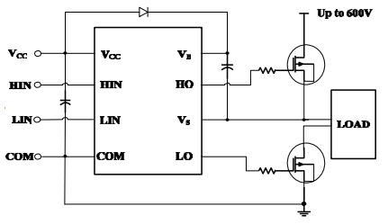
The CXMS5103 is a high voltage, high speed power MOSFET and IGBT driver based on P_SUB P_EPI process. The floating channel driver can be used to drive two N-channel power MOSFET or IGBT independently which operates up to 600V. Logic inputs are compatible with standard CMOS or LSTTL output, down to 3.3V logic. The output drivers feature a high pulse current buffer stage designed for minimum driver cross -conduction. Propagation delays are matched to simplify use in high frequency applications.
-
[ CXMS5103 ]"
目录
7.相关产品
产品概述 返回TOP
The CXMS5103 is a high voltage, high speed power MOSFET and IGBT driver based on P_SUB P_EPI process. The floating channel driver can be used to drive two N-channel power MOSFET or IGBT independently which operates up to 600V. Logic inputs are compatible with standard CMOS or LSTTL output, down to 3.3V logic. The output drivers feature a high pulse current buffer stage designed for minimum driver cross -conduction. Propagation delays are matched to simplify use in high frequency applications.
产品特点 返回TOP
Fully operational to +600 V
3.3 V logic compatible
dV/dt Immunity ±50 V/nsec
Floating channel designed for bootstrap operation
Gate drive supply range from 10 V to 20 V
UVLO for low side channel Output Source / Sink Current Capability 300 mA / 600mA
Independent Logic Inputs to Accommodate All Topologies
-5V negative Vs ability
Matched propagation delay for both channels Patent Pending
应用范围 返回TOP
Small and medium- power motor driver
技术规格书(产品PDF) 返回TOP
需要详细的PDF规格书请扫一扫微信联系我们,还可以获得免费样品以及技术支持!

产品封装图 返回TOP


电路原理图 返回TOP
相关芯片选择指南 返回TOP 更多同类产品.....
| 半桥输出大功率MOS管/IGBT驱动IC | |||||||||
| 型号 | 工作电压 | 静态电流 | I/O拉电流 | I/O灌电流 | 上升时间 | 下降时间 | 开延时 | 关延时 | 封装 |
| CXMS5101B | 10V-20V/高端工作电压120V | 150uA | 0.45A | 0.9A | 70nS | 60nS | 120nS | 120nS | SOP8 |
| CXMS5101 | 11V-30V/高端工作电压100V | 4.5mA | 0.8A | 1A | 400nS | 200nS | 300nS | 400nS | SOP8 |
| CXMS5102 | 11V-30V/高端工作电压100V | 4.5mA | 0.8A | 1A | 400nS | 200nS | 300nS | 400nS | SOP8 |
| CXMS5102B | 10V-20V/高端工作电压600V | 150uA | 0.3A | 0.6A | 60nS | 35nS | 500nS | 500nS | SOP8 |
| CXMS5103 | 10V-20V/高端工作电压600V | 150uA | 0.3A | 0.6A | 90nS | 40nS | 20nS | 20nS | SOP8 |
| 单通道大功率MOS管/IGBT驱动IC | |||||||||
| 型号 | 工作电压 | 静态电流 | I/O拉电流 | I/O灌电流 | 上升时间 | 下降时间 | 开延时 | 关延时 | 封装 |
| CXMS5104 | 3V-30V | 2mA | 1A | 1.2A | 80nS | 20nS | 200nS | 80nS | SOP8 |


