The CXLB7411 is highly-integrated switch-mode system power management devices for smart power bank application and regulated output voltage including 5V /9V /12V. Its low impedance power switch optimizes switch-mode operation efficiency, reduces MOS power consumption. The USB D+/D- data line makes the device protocol handshake to set suitable output voltage to do fast charging function. The chip is compliant with QC 2.0 class A specifications with Max. output current up to 3A at 5V. Besides the converter includes two switch MOSFETs as synchronous boost converter. So no external Schottky diode is required and could get better efficiency near 92%. Other features include built-in soft start, thermal shutdown protection, under-voltage lockout (UVLO), and short circuit protection function, which can shut off the device if output voltage reaches below 1.5V. The CXLB7411 is available in a space-saving SOP-8 (Exposed Pad) package with an exposed pad.
-
[ CXLB7411 ]"
目录
7.相关产品
产品概述 返回TOP
The CXLB7411 is highly-integrated switch-mode system power management devices for smart power bank application and regulated output voltage including 5V /9V /12V. Its low impedance power switch optimizes switch-mode operation efficiency, reduces MOS power consumption. The USB D+/D- data line makes the device protocol handshake to set suitable output voltage to do fast charging function. The chip is compliant with QC 2.0 class A specifications with Max. output current up to 3A at 5V. Besides the converter includes two switch MOSFETs as synchronous boost converter. So no external Schottky diode is required and could get better efficiency near 92%. Other features include built-in soft start, thermal shutdown protection, under-voltage lockout (UVLO), and short circuit protection function, which can shut off the device if output voltage reaches below 1.5V. The CXLB7411 is available in a space-saving SOP-8 (Exposed Pad) package with an exposed pad.
产品特点 返回TOP
● Input Voltage Range from 2.9V to 5.5V.
● Output Voltage Can be Set to 5V/9V/12V.
● Built-in Low RDS(ON) Integrated Power MOSFET NMOS 39mΩ/PMOS 42mΩ
● 3.0A Output Current at 5V
● Fixed Switching Frequency 500KHz .
●±2% Voltage Accuracy
● Power-Save Mode for Light-Load Efficiency.
● Short Circuit Current Fold-back Protection.
● Built-in Soft Start, Output Overvoltage Protection and Thermal Protection
●Supports USB DCP Shorting D+ Line to D- Line per USB Battery Charging Specification, Revision 1.2.
● Meets Chinese Telecommunication Industrial Standard YD/T 1591-2009
● Supports USB DCP applying 2.7V on D+ line and 2.7V on D- line.
● Supports USB DCP applying 1.2V on D+ and Dlines
● Automatic selection of D+/D- mode for an attached device
● Complaint with Apple® and Samsung devices
● SOP-8 (Exposed Pad) Pb-Free Package
应用范围 返回TOP
● Backup Battery Pack
● Mobile / Tablet Power
●Digital Cameras and Bluetooth Accessories
● USB Power Output Ports
技术规格书(产品PDF) 返回TOP
需要详细的PDF规格书请扫一扫微信联系我们,还可以获得免费样品以及技术支持!

产品封装图 返回TOP


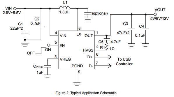
电路原理图 返回TOP
相关芯片选择指南 返回TOP 更多同类产品......
|
QC2.0协议USB快充接口IC |
|||||||
|
型号 |
工作电压 |
工作电流 |
默认输出电压 |
输出电压 |
工作温度范围 |
封装 |
|
|
3.8-6.0V |
60uA |
5V |
5V/9V/12V/20V |
-40--80℃ |
SOP-8 |
||
|
带QC2.0接口的同步DC-DC升压IC |
|||||||||||
|
型号 |
工作 模式 |
工作 电压 范围 |
输出 电压 |
输出电 压形式 |
输出 电压 精度 |
输出 电流 限制 |
效率 |
静态 电流 |
工作 频率 |
封装 |
特点 |
|
PWM |
2.9V-5.5V |
5V|9V|12V |
可调 输出 |
+/-2% |
3A |
91% |
70uA |
500KHz |
ESOP8 |
带QC2.0接口功能(包含了USB智能识别接口功能)内置8A场效应管,单节锂电输入,输出电压可自动识别负载实现5V/3A和9V/1.2A和12V/1A输出, 带使能端,适合QC2.0快充移动电源应用。 |
|
|
带QC2.0接口的高压同步DC-DC降压IC |
||||||||||
|
型号 |
输入 耐压 |
输出 电压 |
输出 电流 |
反馈 电压 |
工作 频率 |
效率 |
静态工 作电流 |
待机 电流 |
封装 |
特点 |
|
10V-35V |
可调 输出 |
2.5A |
0.5V |
130KHz |
93% |
15mA |
50uA |
SOP8 |
带QC2.0接口功能(包含了USB智能识别 接口功能),输出电压可自动识别负载 实现5V/2.5A和9V/1.2A和12V/1A输出。 带CC/CV模式,支持充苹果/三星设 备,适合QC2.0快充车充应用 |
|


