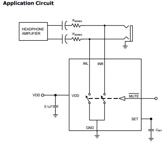
The CXES4274 is an audio click-and-pop eliminator for portable multimedia devices. Operating from a 1.7V to 3. 6V supply, the CXES4274 connects to the output of the existing system amplifier and provides a low-impedance path to ground during startup and shutdown. The inputs INL and INR accept voltage swings from VDD to 5.5V below VDD
-
[ CXES4274 ]"
目录
7.相关产品
产品概述 返回TOP
The CXES4274 is an audio click-and-pop eliminator for portable multimedia devices. Operating from a 1.7V to 3. 6V supply, the CXES4274 connects to the output of the existing system amplifier and provides a low-impedance path to ground during startup and shutdown. The inputs INL and INR accept voltage swings from VDD to 5.5V below VDD. See the Setting the Supply Voltage section for more information. The power-up and power down transients are shunted to ground to prevent clicks and pops from becoming audible. The CXES4274 features two low-impedance analog switches controlled by MUTE that opens and closes the switches. The switches are open during normal operation and have no impact on the output signal.During startup and shutdown of the amplifier, the CXES4274 can be activated to short the outputs to ground and prevent clicks and pops from pulling current through the headphones.
产品特点 返回TOP
· Wide supply voltage range from 1.7V to 3.6V
· Low quiescent current 1mA
· Adjustable turn off time by SET pin
· Fast turn on time : 100us(typ)
· Low switch resistance :0.3W
· Distortion-Free, Click-and-Pop Elimination
· Available in WLCSP1.42x0.92 - 6 Packages
· Lead Free Green Devices Available (RoHS Compliant)
应用范围 返回TOP
· Smart Phones
· Tablet PCs
· Portable Media Players
技术规格书(产品PDF) 返回TOP
需要详细的PDF规格书请扫一扫微信联系我们,还可以获得免费样品以及技术支持!

产品封装图 返回TOP


电路原理图 返回TOP


相关芯片选择指南 返回TOP 更多同类产品......
|
Products > Switch > Power Distribution Controller |
|||||||||||||||
|
Part_No |
Package |
No.of Channel |
External Power Switch Type |
Input Voltage (V) |
Quescint Current (uA) |
Wrong Input Voltage Protection |
Inpute Voltage UVLO |
SCP |
OCP (A) |
OVP |
UVP |
EN |
High/ Low EN |
POK |
|
|
min |
max |
||||||||||||||
|
SOP8 TDFN2x2-8 |
1 |
N-Channel MOSFET |
10 |
26 |
750 |
Y |
Y |
Y |
Y |
Y |
Y |
Y |
H |
Y |
|
|
TDFN3x3-10 |
1 |
N-Channel MOSFET |
5 |
26 |
500 |
Y |
Y |
Y |
Y |
Y |
Y |
H |
Y |
||
|
TDFN3x3-10 |
1 |
N-channel MOSFET |
5 |
26 |
500 |
Y |
Y |
Y |
Y |
Y |
Y |
H |
Y |
||
|
Switch> Analog Switch |
||||||||
|
Part_No |
Package & Pins |
VDD Voltage (V) |
IDD, Supply Current (mA) |
Input Voltage (max)(V) |
Power Switch On Resistance(milohm) |
Turn-On Time(ms) |
Turn-Off Time(ms) |
|
|
min |
max |
|||||||
|
WLCSP1.2x1.2-9 |
2.9 |
5.5 |
35 |
0~5.5 |
0.2 |
5 |
1 |
|
|
WLCSP1.2x0.8-6 |
1.5 |
5.5 |
20 |
1.5-5.5 |
22 |
4.4 |
36.5 |
|
|
WLCSP 1.42x0.92-6 |
1.7 |
3.6 |
0.5 |
VDD-5.5~VDD |
0.2 |
0.1 |
1 |
|
|
Switch> DrMOS |
||||||||||||||
|
Part_No |
Package |
Description |
Topology |
# of PWM Outputs |
Drive Lout (A) |
Vin (V) |
Fmax (Khz) |
R-Top (milohm) |
R-Sync (milohm) |
Iq (No load) (uA) |
En pin |
Sync Pin |
PSM/ CCM pin |
|
|
min |
max |
|||||||||||||
|
TQFN4 x4-23P |
High-Performance, High-Current DrMOS Power Module |
high/Low-sideN-channel MOSFET |
1 |
8 |
4.5 |
25 |
1500 |
25 |
7 |
90 |
Y |
N |
Y |
|
|
TQFN4x4 -23P |
High-Performance, High-Current DrMOS Power Module |
high/Low-sideN-channel MOSFET |
1 |
6 |
4.5 |
25 |
1500 |
30 |
12 |
90 |
Y |
N |
Y |
|
|
TQFN5 x5-30 |
High-Performance,High-Current DrMOS Power Module |
high/Low-sideN-channel |
MOSFET1 |
13 |
4.5 |
25 |
1500 |
9.7 |
5.2 |
90 |
Y |
N |
Y |
|
|
TQFN5 x5-30 |
High-Performance,High-Current DrMOS Power Module |
high/Low-sideN-channel MOSFET |
1 |
15 |
4.5 |
25 |
1500 |
8 |
4.5 |
90 |
Y |
N |
Y |
|
|
TQFN5 x5-30 |
High-Performance,High-Current DrMOS Power Module |
high/Low-sideN-channel MOSFET |
1 |
15 |
4.5 |
25 |
1500 |
8 |
4.5 |
90 |
Y |
N |
Y |
|


