The CX8PU86LV CXUS7719 has program memory size greater 2K works, but the CALL and GOTO instructions only have a 11-bits address range. This 11-bit address range allows a branch within a 2K program memory page size. To allow CALL and GOTO instructions to address the entire 6K program memory address range for CX8PU86LV CXUS7719, there is another two bits to specify the program memory page. The paging bit comes from the ROMBANK[1:0] bits(PUMODE[6:5]). When doing a CALL or GOTO instruction, the user must ensure that page bit ROMBANK[1:0] are programmed so that the desired program memory page is addressed. When one of return instructions is executed, the entire 13-bit PC is POPed from the stack. Therefore, manipulation of the ROMBANK[1:0] is not required for return instructions
-
[ CXUS7718 ]"
目录
1.产品概述 2.产品特点 3.应用范围 4.技术规格书下载(PDF文档)
一.产品概述
The CX8PU86LV CXUS7719 has program memory size greater 2K works, but the CALL and GOTO instructions only have a 11-bits address range. This 11-bit address range allows a branch within a 2K program memory page size. To allow CALL and GOTO instructions to address the entire 6K program memory address range for CX8PU86LV CXUS7719, there is another two bits to specify the program memory page. The paging bit comes from the ROMBANK[1:0] bits(PUMODE[6:5]). When doing a CALL or GOTO instruction, the user must ensure that page bit ROMBANK[1:0] are programmed so that the desired program memory page is addressed. When one of return instructions is executed, the entire 13-bit PC is POPed from the stack. Therefore, manipulation of the ROMBANK[1:0] is not required for return instructions
二.产品特点
USB Specification Compliance
Support Full-Speed and Low-Speed USB 2.0 specification.
Built-in USB Transceiver.
Built-in 1.5k pull-high resistor.
Support one address and four 8-byte and two 32-byte data endpoints.
Support USB Suspend and Resume function.
One Control IN/OUT endpoints, two INT,BULK endpoints.
8-bit RISC microprocessor
6K x 14 internal program OTP-ROM.
256 bytes internal SRAM.
Optional 12MHz/24MHz internal MCU clock by configuration.
Optional Default/16MHz/12MHz/6MHz/58KHz internal MCU clock by firmware.
One Watch dog Timer ,Timer0,Timer1,and two captures Timers.
System Clock
Internal Oscillator
Internal +/- 4% 24MHz Oscillator
0.25% Accuracy after USB traffic is received.
Internal slow oscillator 58KHz free run clock for suspend mode.
Built-in flexible programming PLL for external Oscillator or crystal
Operating Frequency Range of Oscillator/crystal is 2~48 MHz.
Optional external ceramic resonator or internal clock mode..16-I/O ports
High current drive on any GPIO pin : 25mA/pin current sink.
Each GPIO pin supports high-impedance input, internal pull-ups,
open drains output, or CMOS outputs.
Power Manager and consumption
Power on reset (POR) is 2.0V
Chip can work on greater than 2.2V power.
Low Voltage Detect is 3.8V
Regulator 3.3V output, supply 45mA current.
MCU operating at 24MHz clock
Enable USB operating current is 17mA as Vcc=5V.
Disable USB operating current is 6mA as Vcc=3.3V.
MCU operating at 12MHz clock
Enable USB operating current is 13mA as Vcc=5V.
Disable USB operating current is 4mA as Vcc=3.3V
GPIO supply 1.8V~5V interface.
Support SSC to reduce EMI.
三.应用范围
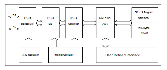
The CX8PU86LV CXUS7719 is an 8-bit microprocessor embedded device tailored to the
USB application. It includes an 8-bit RISC CPU core, 192~256 byte SRAM, Full Speed and
Low Speed USB Interface and a 6K x 14 internal program OTP-ROM.
四.技术规格书(产品PDF)
需要详细的PDF规格书请扫一扫微信联系我们,还可以获得免费样品以及技术支持!

五.产品封装图

六.电路原理图
七.相关芯片选择指南 更多同类产品......
|
USB |
|||||||||||||||||
|
Product Name |
OTP |
RAM |
I/O |
I/O |
3.3V |
USB |
Stack |
EP0 |
EP1 |
EP2 |
EP3 |
EP4 |
|||||
|
ROM |
Byte |
Voltage |
OUT |
MODE |
|||||||||||||
|
Range |
IN |
OUT |
IN |
OUT |
IN |
OUT |
IN |
OUT |
IN |
OUT |
|||||||
|
4K(OTP) |
192 |
14 |
1.8V~5.5V |
45mA |
INT/BULK |
8 |
64Byte |
64Byte |
64Byte |
64Byte |
64Byte |
64Byte |
64Byte |
64Byte |
NA |
NA |
|
|
6K(OTP) |
192 |
16 |
1.8V~5.5V |
45mA |
INT/BULK |
5 |
8Byte |
8Byte |
8Byte |
NA |
8Byte |
NA |
32Byte |
NA |
NA |
32Byte |
|
|
6K(OTP) |
192 |
16 |
1.8V~5.5V |
45mA |
INT/BULK |
5 |
8Byte |
8Byte |
8Byte |
NA |
8Byte |
||||||


