The CXSB6611 series is a 2 channel (step-up and inverting) DC/DC converter IC. One DC/DC converter is a step-up DC/DC and the other is an inverting DC/DC converter. The step-up converter compares a built-in reference voltage 1.0V to the FBP voltage (accuracy ±1.5%) and a positive output voltage can be set freely with the external components up to 18V. The inverting DC/DC converter compares a difference between a reference voltage and the FBN voltage (accuracy ±1.5%) to the GND, then a negative output voltage can be set until -15V with the external components. With a 1.2MHz frequency, the size of the external components can be reduced. As for operation mode, the device can be selected to use PWM control or automatic PWM/PFM switching control by the MODE pin. In the automatic PWM/PFM switching control mode, control switches from PWM to PFM during light loads. The series is highly efficient from light loads through to large output currents. In the PWM control mode, noise is easily reduced since the frequency is fixed. The control mode can be selected for each application. The soft start and current control functions are internally optimized. During stand-by, all circuits in the IC are shutdown to reduce current consumption to as low as 1.0μA or less. The device includes a gate control pin for the P-channel MOSFET which is used for a load disconnection at the stand-by mode. The GAINP and GAINN pins are used for loop compensation in order to optimize load transient response. With the built-in UVLO (Under Voltage Lock Out) function, the internal driver transistor is forced OFF when input voltage becomes 2.2V or lower.
-
"
| Content | |||||||||||||||||||||||||||||||||||||||||||||||||||||||||||||||||||||||||||||||||||||||||||||||||||||||||||||||||||||||||||
|---|---|---|---|---|---|---|---|---|---|---|---|---|---|---|---|---|---|---|---|---|---|---|---|---|---|---|---|---|---|---|---|---|---|---|---|---|---|---|---|---|---|---|---|---|---|---|---|---|---|---|---|---|---|---|---|---|---|---|---|---|---|---|---|---|---|---|---|---|---|---|---|---|---|---|---|---|---|---|---|---|---|---|---|---|---|---|---|---|---|---|---|---|---|---|---|---|---|---|---|---|---|---|---|---|---|---|---|---|---|---|---|---|---|---|---|---|---|---|---|---|---|---|---|
目录7.相关产品 产品概述 返回TOP CXSB6611系列产品是升压,反转的DC/DC转换器。2个DC/DC转换器中,1个作为升压DC/DC转换器,另一个作为反转的DC/DC转换器。升压DC/DC转换器通过内部1.0V的标准参考电压,使用外部电阻, 输出电压可以在4.0V~18.0V的范围内自由设定。反转的DC/DC转换器,输出电压可以在-15.0V~-4.0V的范围内自由设定。开关频率高达1.2MHz,可使用小尺寸的外围器件。用MODE引脚能从PWM控制与PWM/PFM自动切换控制中任意选择工作模式。PWM/PFM自动切换方式, 能从轻负载到高负载整个负载范围内的高效率。由于PWM控制固定了开关频率,能轻易滤除噪声。因此可以选择最合适的工作模式。在内部实施了软启动功能和限流功能的最佳化。由于在待机时整个电路停止工作,能把消耗电流抑制在1.0μA以下。内置了负载切断功能,由于外置了P沟道MOSFET,能在停机时切断负载。为了达到最佳负载瞬态响应,能调节GAINP引脚和GAINN引脚,进行外部补偿。内置了UVLO (输入欠压锁闭Under Voltage Lock Out) 功能,在输入电压低于2.2V时,能强制停止内部驱动晶体管工作。The CXSB6611 series is a 2 channel (step-up and inverting) DC/DC converter IC. One DC/DC converter is a step-up DC/DC and the other is an 产品特点 返回TOP
应用范围 返回TOP ●AMOLED - Smartphones - Tablet PCs - Automotive navigation systems ●CCD image sensors - Surveillance cameras ●e-paper 技术规格书(产品PDF) 返回TOP 需要详细的PDF规格书请扫一扫微信联系我们,还可以获得免费样品以及技术支持! 产品封装图 返回TOP
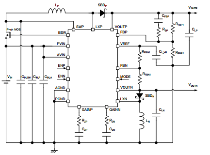
电路原理图 返回TOP |


|
多通道型DC/DC转换器 |
|||||||||||||
|
产品名称 |
特点/类型 |
封装 |
控制 |
VIN MIN |
VIN MAX |
VOUT MIN |
VOUT MAX |
IOUT IIN |
FB/VOUT 电压精度 |
振荡频率 |
限制 电流 |
消耗 电流 |
温度范围 |
|
(V) |
(V) |
(V) |
(V) |
mA |
% |
kHz |
A |
μA |
℃ |
||||
|
升压+升压 |
MSOP10 USP10 |
PWM/PFM |
0.9 |
10 |
1.5 |
30 |
500 |
±2.0 |
100,180, 300,500 |
70 |
-40~+85 |
||
|
升压+降压 |
MSOP10 USP10 |
PWM/PFM |
2 |
10 |
1.5 |
30 |
500 |
±2.0 |
100,300,500 |
70 |
-40~+85 |
||
|
降压+降压 |
MSOP10 USP10 |
PWM/PFM |
2 |
10 |
0.9 |
6 |
1000 |
±2.0 |
100,300,500 |
60 |
-40~+85 |
||
|
升压+反转 |
MSOP10 USP10 |
PWM/PFM |
2 |
10 |
1.5 |
30 |
500 |
±2.0 |
100,300,500 |
90 |
-40~+85 |
||
|
降压+反转 |
MSOP10 USP10 |
PWM/PFM |
2 |
10 |
0.9 |
6 |
1000 |
±2.0 |
100,300,500 |
80 |
-40~+85 |
||
|
2ch降压+电 压检测器 |
QFN20 |
PWM |
2.5 |
5.5 |
1.2 |
4 |
800 |
±2.0 |
1000 |
1 |
950 |
-40~+85 |
|
|
升压+电压泵x2 |
QFN20 |
PWM |
2.5 |
5.5 |
5.5 |
19 |
500 |
±1.5 |
ADJ |
1.1 |
2 |
-40~+85 |
|


