CXAS42272 Several Protection features include current limiting with foldback, and thermal shutdown to prevent catastrophic switch failure caused by increasing power dissipation when continuous heavy loads or short circuit occurs. A built-in charge pump is used to drive the N-channel MOSFET that is free of parasitic body diode to eliminate any reversed current flow across the switch when it is powered off
-
[ CXAS42272 ]"
目录
7.相关产品
产品概述 返回TOP
Several Protection features include current limiting with foldback, and thermal shutdown to prevent catastrophic switch failure caused by increasing power dissipation when continuous heavy loads or short circuit occurs. A built-in charge pump is used to drive the N-channel MOSFET that is free of parasitic body diode to eliminate any reversed current flow across the switch when it is powered off. OC is open-drain output report over-current or over-temperature event and has typical 9ms deglitch timeout period.The CXAS42272 is an integrated power switch for self-powered. The CXAS42272 has a typical RDS(ON) of 70mohm.
产品特点 返回TOP
„ 70mΩ High-Side MOSFET
„ Internal Current Limit to 3.3A (TYP)
„ Operating Range:2.7V to 5.5V
„ 1mS Typical Rise Time
„ Fast Overcurrent Response:3μS (TYPICAL)
„ Under voltage Lockout
„ 100μA Quiescent Supply Current
„ 1μA Maximum Shutdown Supply Current
„ Logic Level Enable Pin, Available with Active-High or Active-Low Version
„ No Reverse Current when Power Off
„ Deglitched Open-Drain Over-Current Flag Output ( OC )
„ MSOP-8 Package
应用范围 返回TOP
„ High-Side Power Protection Switch
„ USB Power Management
„ Hot Plug-In Power Supplies
„ Battery-Charger Circuits
技术规格书(产品PDF) 返回TOP
需要详细的PDF规格书请扫一扫微信联系我们,还可以获得免费样品以及技术支持!

产品封装图 返回TOP

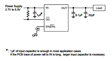
电路原理图 返回TOP
相关芯片选择指南 返回TOP 更多同类产品......
|
Single Power Switch |
|||||||||
|
Part NO. |
Vin(V) min. |
Vin(V) max. |
RON (Ohm) |
VOUT rising (μs) |
Ilimit (A) |
OC Flag |
Discharge (Ohm) |
Note |
Package |
|
1 |
3.6 |
25 |
140 |
1 |
N |
80 |
RON = 56m ohm@VIN = 1.2V |
WLCSP2X2-4 |
|
|
1 |
3.6 |
78 |
48/220 |
0.5 |
N |
88/N |
RON = 146m ohm@VIN = 1.2V |
WLCSP2X2-4 |
|
|
1.5 |
5 |
25 |
130 |
3 |
N |
250 |
RON = 68m ohm@VIN = 1.5V |
WLCSP2X2-4 |
|
|
1.5 |
5.5 |
20 |
3300 |
3 |
N |
N |
RON = 48m ohm@VIN = 1.5V |
WLCSP2X3-6 |
|
|
0.6 |
5.5 |
12 |
ADJ |
12 |
N |
150 |
HV Vbias Needs |
ADFN2X2-8 |
|
|
2.7 |
5.5 |
120 |
150 |
2 |
N |
75 |
N/A |
SOT-23-5 |
|
|
2.7 |
5.5 |
120 |
1900 |
2 |
N |
75 |
SS |
SOT-23-5 |
|
|
2.7 |
5.5 |
120 |
1900 |
2.5 |
N |
R |
SS,External discharging |
SOT-23-5/ADFN1.5X1.5-6 |
|
|
2.7 |
5.5 |
70 |
1400 |
1 |
Y |
130 |
N/A |
SOT-23-5 |
|
|
2.7 |
5.5 |
90 |
1200 |
ADJ |
-- |
-- |
-- |
SOT-23-5 |
|
|
2.7 |
5.5 |
90 |
1500 |
ADJ |
Y |
N |
SS, OC Setting by a R |
SOP-8/TDFN2X2-6/ MSOP-8 |
|
|
2 |
5.5 |
80 |
2500 |
2.5 |
N |
153 |
Turn on delay 800us |
TDFN2X2-8 |
|
|
2 |
5.5 |
85 |
1500 |
2.5 |
N |
153 |
Turn on delay 800us |
SOT-23-5 |
|
|
1.5 |
5.5 |
80 |
1000 |
-- |
N |
R |
External discharging |
TDFN1.6X1.6-6 |
|
|
2.7 |
5.5 |
70 |
1000 |
1.2 |
Y |
N |
SS, Fast SCP, HML 2.0 VOUT Reverse-Voltage Protection |
SOT-23-6 |
|
|
2.7 |
5.5 |
70 |
1000 |
3.3 |
Y |
N |
N/A |
MSOP-8 |
|
|
2.7 |
5.5 |
70 |
1000 |
1.5 |
Y |
N |
N/A |
SOP-8 |
|
|
2.7 |
5.5 |
125 |
1500 |
0.45 |
Y |
75 |
N/A |
SOP-8 |
|
|
2.7 |
5.5 |
70 |
1500 |
2.5 |
Y |
70 |
N/A |
SOP-8/MSOP-8/ TDFN3X3-8 |
|
|
0.6 |
5.5 |
5.5 |
ADJ |
10 |
N |
150 |
Need a 5V Bbias, A/B/C = 5.5/11/22 m ohm; 10A/6A/4A |
TDFN3X3-8/MSOP-8(FD)/SOT-23-6 |
|


