The CXAS42268 operates with an input voltage ranging from 2V to 5.5V. It is suitable for both 3V and 5V systems. The CXAS42268 also features an under voltage lock out which turns the switch off when an input under-voltage condition exists. Input logic levels are TTL and 2.5V to 5V CMOS compatible.
-
[ CXAS42268 ]"
目录
7.相关产品
产品概述 返回TOP
The CXAS42268 operates with an input voltage ranging from 2V to 5.5V. It is suitable for both 3V and 5V systems. The CXAS42268 also features an under voltage lock out which turns the switch off when an input under-voltage condition exists. Input logic levels are TTL and 2.5V to 5V CMOS compatible. In shutdown mode, the supply current decreases to less than 1μA.The CXAS42268 is available in a 8 pin TDFN package.The CXAS42268is a N-channel MOSFET power switch designed for high-side load-switching applications, and the device has a typical RDS(ON) of 80m and the output current is limited to 2A.The CXAS42268has a slew rate limited turnon load switch and offers a shutdown load discharge circuit to rapidly turn off a load circuit when the switch is disabled.
产品特点 返回TOP
„ 2.0V to 5.5V Input Voltage Range
„ Very Low RDS(ON) , Typically 80m. (5V)
„ Typical Current Limited is 2.5A at VCC=5V
„ Slew Rate Limited Turn-On Time 1.5ms (5V)
„ Fast Shutdown Load Discharge
„ TTL/CMOS Input Logic Level
„ No Reverse Output Current
„ 8 Pin TDFN Package
应用范围 返回TOP
„ Cellular Telephones
„ Digital Still Cameras
„ Hot Swap Supplies
„ Notebook Computers
„ Personal Communication Devices
„ Personal Digital Assistants (PDAs)
技术规格书(产品PDF) 返回TOP
需要详细的PDF规格书请扫一扫微信联系我们,还可以获得免费样品以及技术支持!

产品封装图 返回TOP

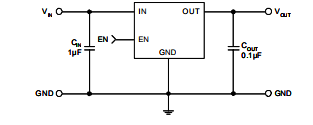
电路原理图 返回TOP
相关芯片选择指南 返回TOP 更多同类产品......
|
Single Power Switch |
|||||||||
|
Part NO. |
Vin(V) min. |
Vin(V) max. |
RON (Ohm) |
VOUT rising (μs) |
Ilimit (A) |
OC Flag |
Discharge (Ohm) |
Note |
Package |
|
1 |
3.6 |
25 |
140 |
1 |
N |
80 |
RON = 56m ohm@VIN = 1.2V |
WLCSP2X2-4 |
|
|
1 |
3.6 |
78 |
48/220 |
0.5 |
N |
88/N |
RON = 146m ohm@VIN = 1.2V |
WLCSP2X2-4 |
|
|
1.5 |
5 |
25 |
130 |
3 |
N |
250 |
RON = 68m ohm@VIN = 1.5V |
WLCSP2X2-4 |
|
|
1.5 |
5.5 |
20 |
3300 |
3 |
N |
N |
RON = 48m ohm@VIN = 1.5V |
WLCSP2X3-6 |
|
|
0.6 |
5.5 |
12 |
ADJ |
12 |
N |
150 |
HV Vbias Needs |
ADFN2X2-8 |
|
|
2.7 |
5.5 |
120 |
150 |
2 |
N |
75 |
N/A |
SOT-23-5 |
|
|
2.7 |
5.5 |
120 |
1900 |
2 |
N |
75 |
SS |
SOT-23-5 |
|
|
2.7 |
5.5 |
120 |
1900 |
2.5 |
N |
R |
SS,External discharging |
SOT-23-5/ADFN1.5X1.5-6 |
|
|
2.7 |
5.5 |
70 |
1400 |
1 |
Y |
130 |
N/A |
SOT-23-5 |
|
|
2.7 |
5.5 |
90 |
1200 |
ADJ |
-- |
-- |
-- |
SOT-23-5 |
|
|
2.7 |
5.5 |
90 |
1500 |
ADJ |
Y |
N |
SS, OC Setting by a R |
SOP-8/TDFN2X2-6/ MSOP-8 |
|
|
2 |
5.5 |
80 |
2500 |
2.5 |
N |
153 |
Turn on delay 800us |
TDFN2X2-8 |
|
|
2 |
5.5 |
85 |
1500 |
2.5 |
N |
153 |
Turn on delay 800us |
SOT-23-5 |
|
|
1.5 |
5.5 |
80 |
1000 |
-- |
N |
R |
External discharging |
TDFN1.6X1.6-6 |
|
|
2.7 |
5.5 |
70 |
1000 |
1.2 |
Y |
N |
SS, Fast SCP, HML 2.0 VOUT Reverse-Voltage Protection |
SOT-23-6 |
|
|
2.7 |
5.5 |
70 |
1000 |
3.3 |
Y |
N |
N/A |
MSOP-8 |
|
|
2.7 |
5.5 |
70 |
1000 |
1.5 |
Y |
N |
N/A |
SOP-8 |
|
|
2.7 |
5.5 |
125 |
1500 |
0.45 |
Y |
75 |
N/A |
SOP-8 |
|
|
2.7 |
5.5 |
70 |
1500 |
2.5 |
Y |
70 |
N/A |
SOP-8/MSOP-8/ TDFN3X3-8 |
|
|
0.6 |
5.5 |
5.5 |
ADJ |
10 |
N |
150 |
Need a 5V Bbias, A/B/C = 5.5/11/22 m ohm; 10A/6A/4A |
TDFN3X3-8/MSOP-8(FD)/SOT-23-6 |
|


