CXES4271A CXES4271 is a high-side power distribution controller for an external N-channel MOSFET, allow for +12V, +19V or +5V power-supply rail. The wrong input voltage protection function protects a wrong input adapter insertion, when input voltage is out of the target input voltage range the IC is off. The over-current protection monitors the output current by using the voltage drop across the external sensing resistor, when output current reaches the trip point the IC will be shut down
-
[ CXES4271 ]"
目录
7.相关产品
产品概述 返回TOP
CXES4271A CXES4271 is a high-side power distribution controller for an external N-channel MOSFET, allow for +12V, +19V or +5V power-supply rail. The wrong input voltage protection function protects a wrong input adapter insertion, when input voltage is out of the target input voltage range the IC is off. The over-current protection monitors the output current by using the voltage drop across the external sensing resistor, when output current reaches the trip point the IC will be shut down. The CXES4271A CXES4271 also provides a shortcircuit protection during power-up. The device monitors VOUT voltages for a short-circuit detection, if a short-circuit condition is detected the IC will be shut down. Other features include a POK output to indicate the output voltage is ready, and a logic-controlled shutdown mode.
产品特点 返回TOP
· High-Side Driver for an External N-Channel MOSFET
· Under-Voltage Lockout (UVLO)
· Wrong VIN Input Voltage Protection
· Output Under-Voltage Protection (UVP)
· Short-Circuit Protection During Power-up (SCP)
· Over-Current Protection (OCP)
· Selectable VIN Monitor Voltage
· Shutdown Function
· Power Okay (POK) Function
· Lead Free and Green Devices Available (RoHS Compliant)
应用范围 返回TOP
· AIO Computers
· Notebooks
技术规格书(产品PDF) 返回TOP
需要详细的PDF规格书请扫一扫微信联系我们,还可以获得免费样品以及技术支持!

产品封装图 返回TOP


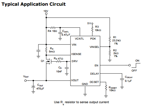
电路原理图 返回TOP

相关芯片选择指南 返回TOP 更多同类产品......
|
Products > Switch > Power Distribution Controller |
|||||||||||||||
|
Part_No |
Package |
No.of Channel |
External Power Switch Type |
Input Voltage (V) |
Quescint Current (uA) |
Wrong Input Voltage Protection |
Inpute Voltage UVLO |
SCP |
OCP (A) |
OVP |
UVP |
EN |
High/ Low EN |
POK |
|
|
min |
max |
||||||||||||||
|
SOP8 TDFN2x2-8 |
1 |
N-Channel MOSFET |
10 |
26 |
750 |
Y |
Y |
Y |
Y |
Y |
Y |
Y |
H |
Y |
|
|
TDFN3x3-10 |
1 |
N-Channel MOSFET |
5 |
26 |
500 |
Y |
Y |
Y |
Y |
Y |
Y |
H |
Y |
||
|
TDFN3x3-10 |
1 |
N-channel MOSFET |
5 |
26 |
500 |
Y |
Y |
Y |
Y |
Y |
Y |
H |
Y |
||
|
Switch> Analog Switch |
||||||||
|
Part_No |
Package & Pins |
VDD Voltage (V) |
IDD, Supply Current (mA) |
Input Voltage (max)(V) |
Power Switch On Resistance(milohm) |
Turn-On Time(ms) |
Turn-Off Time(ms) |
|
|
min |
max |
|||||||
|
WLCSP1.2x1.2-9 |
2.9 |
5.5 |
35 |
0~5.5 |
0.2 |
5 |
1 |
|
|
WLCSP1.2x0.8-6 |
1.5 |
5.5 |
20 |
1.5-5.5 |
22 |
4.4 |
36.5 |
|
|
WLCSP 1.42x0.92-6 |
1.7 |
3.6 |
0.5 |
VDD-5.5~VDD |
0.2 |
0.1 |
1 |
|
|
Switch> DrMOS |
||||||||||||||
|
Part_No |
Package |
Description |
Topology |
# of PWM Outputs |
Drive Lout (A) |
Vin (V) |
Fmax (Khz) |
R-Top (milohm) |
R-Sync (milohm) |
Iq (No load) (uA) |
En pin |
Sync Pin |
PSM/ CCM pin |
|
|
min |
max |
|||||||||||||
|
TQFN4x 4-23P |
High-Performance, High-Current DrMOS Power Module |
high/Low-sideN-channel MOSFET |
1 |
8 |
4.5 |
25 |
1500 |
25 |
7 |
90 |
Y |
N |
Y |
|
|
TQFN4x 4-23P |
High-Performance, High-Current DrMOS Power Module |
high/Low-sideN-channel MOSFET |
1 |
6 |
4.5 |
25 |
1500 |
30 |
12 |
90 |
Y |
N |
Y |
|
|
TQFN5x 5-30 |
High-Performance,High-Current DrMOS Power Module |
high/Low-sideN-channel |
MOSFET1 |
13 |
4.5 |
25 |
1500 |
9.7 |
5.2 |
90 |
Y |
N |
Y |
|
|
TQFN5x 5-30 |
High-Performance,High-Current DrMOS Power Module |
high/Low-sideN-channel MOSFET |
1 |
15 |
4.5 |
25 |
1500 |
8 |
4.5 |
90 |
Y |
N |
Y |
|
|
TQFN5x 5-30 |
High-Performance,High-Current DrMOS Power Module |
high/Low-sideN-channel MOSFET |
1 |
15 |
4.5 |
25 |
1500 |
8 |
4.5 |
90 |
Y |
N |
Y |
|


