This ADC requires one point eight V single power supply and LVPECL / CMOS / LVDS compatible sampling clock signal, in order to give full play to its performance. No external reference voltage source or driver is needed to meet many application requirements. The PLL allows the user to provide a single ADC sampling clock. The corresponding jesd204b data rate clock is generated by multiplying the PLL by the ADC sampling clock.

-
[ CXAD33115A ]"
目录
7.相关产品
产品概述 返回TOP
CXAD33115A CXAD33115B是一款4通道、16位、125 MSPS模数转换器(ADC)。该芯片内置采样保持电路,专门针对低功耗、小尺寸和易用性而设计。该产品的转换速率最高可达125 MSPS,具有杰出的动态性能与低功耗特性,适合强调小封装尺寸的应用。 该ADC要求采用1.8 V单电源供电以及LVPECL/CMOS/LVDS兼容型采样时钟信号,以便充分发挥其工作性能。无需外部基准电压源或驱动器件即可满足许多应用需求。 该ADC片内锁相环(PLL)允许用户提供单个ADC采样时钟,对应JESD204B数据速率时钟由PLL乘以该ADC采样时钟产生。 CXAD33115A CXAD33115B具有极低的功耗,正常工作时为832 mW。它还支持独立关断各通道,禁用所有通道时,典型功耗低于5.10 mW。 CXAD33115A CXAD33115B采用符合RoHS标准的56引脚QFN封装,额定温度范围为−45°C至+85°C。
产品特点 返回TOP
最高采样速率:125 MSPS
信噪比(SNR):77.5dBFS @ 10MHz and 125MSPS
无杂散动态范围(SFDR):90dBc @ 10MHz and 125MSPS
中频采样频率可达 300MHz
1.8V 单电源供电
低功耗:796mW (125 MSPS)
1.8V CMOS或LVDS输出
1至8整数输入时钟分频器
集成ADC时钟占空比稳定器
多芯片同步功能
可编程ADC内部基准电压源
灵活的模拟输入范围:1.0V峰峰值至2.0V峰峰值
节能的掉电模式
大于90dB的通道隔离度
串行端口控制
应用范围 返回TOP
a
技术规格书(产品PDF) 返回TOP
需要详细的PDF规格书请扫一扫微信联系我们,还可以获得免费样品以及技术支持!

产品封装图 返回TOP
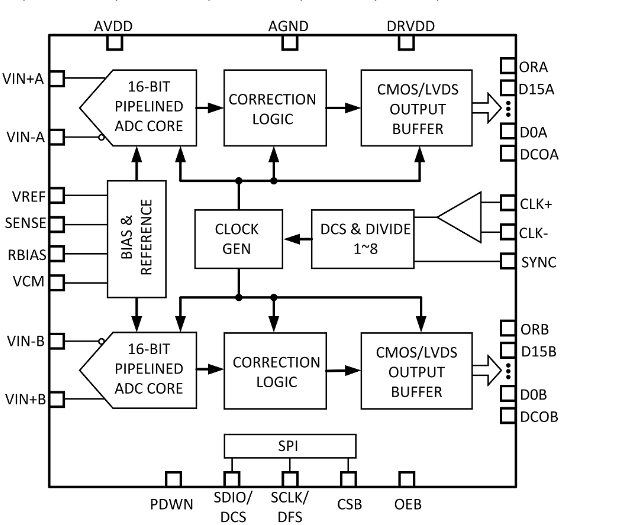
电路原理图 返回TOP
a
相关芯片选择指南 返回TOP 更多同类产品......
|
高速高精度ADC系列(ADC) |
|||||||||||
|
Part No. |
分辨率 |
采样率 |
通道数 |
INL |
DNL |
满幅输入范围 |
SNR |
SFDR |
Power Consumption |
数据 输出接口 |
Package |
|
14bit |
125 |
2 |
±2LSB |
±0.25LSB |
2 |
76dBFS |
>85dBc |
796mW |
CMOS/LVDS |
QFN64 |
|
|
14bit |
155 |
2 |
±2LSB |
±0.25LSB |
2 |
75.5dBFS |
>91dBc |
820mW |
CMOS |
QFN64 |
|
|
14bit |
80 |
2 |
±1.5LSB |
±0.5LSB |
2 |
76.5dBFS |
>88dBc |
477mW |
CMOS/LVDS |
QFN64 |
|
|
14bit |
125 |
4 |
±2LSB |
±0.5LSB |
2 |
76.4dBFS |
>84.4dBc |
580mW |
Serial LVDS |
QFN48 |
|
|
14bit |
80 |
4 |
±1LSB |
±0.4LSB |
2 |
76.6dBFS |
>85.5dBc |
525mW |
Serial LVDS |
QFN48 |
|
|
16bit |
125 |
2 |
±4.5LSB |
±0.5LSB |
2 |
77dBFS |
>90dBc |
796mW |
CMOS/LVDS |
QFN64 |
|
|
16bit |
80 |
2 |
±4.5LSB |
±0.5LSB |
2 |
77.5dBFS |
>90dBc |
477mW |
CMOS/LVDS |
QFN64 |
|
|
16bit |
125 |
4 |
±2.2LSB |
±0.25LSB |
2.8 |
81.1dBFS |
>94.7dBc |
832mW |
JESD204B |
QFN56 |
|
|
16bit |
125 |
4 |
±4.5LSB |
±0.7LSB |
2 |
78.6dBFS |
>90dBc |
630mW |
Serial LVDS |
QFN48 |
|